
SK Telecom said on June 1 that it has put SK hynix’s semiconductor fabs into a digital twin built on NVIDIA Omniverse libraries, with commercialization to follow in stages under SK hynix’s “Autonomous Fab 2030” roadmap. SK hynix’s news is part of a trend involving Omniverse-based fab twins. SK hynix and SKT first surfaced the…
What Apple’s new CEO could mean for its R&D strategy

What happens when the world’s most valuable consumer tech company, which has been spending more than $30B annually on R&D, hands the CEO reins to a mechanical engineer? Starting September 1, Apple will begin answering that question. John Ternus, the 50-year-old hardware chief who joined Apple’s product design team in 2001, will succeed Tim…
Copper is hitting its physical limit with AI. Why NTT thinks photonics is could unblock it.

To say that the chips powering the current AI wave are hot is an understatement. NVIDIA booked $39.1 billion in data center revenue in the first quarter of fiscal 2026, a 73% bump year over year. But they are, of course, also hot physically. The B200, a flagship Blackwell GPU, draws up to 1,000 watts.…
Nanoscale ridges in a substrate add 15 K and 50 Tesla to a superconductor’s limits

Superconducting materials can carry electricity with zero resistance, but two persistent problems have kept them out of most real-world electronics: they need to be cooled to extreme temperatures, and strong magnetic fields tend to destroy the superconducting state. Researchers at Chalmers University of Technology report a new material design strategy that pushes back on both…
Marktech expands large-area silicon photodiode portfolio for spectroscopy, medical diagnostics
Marktech Optoelectronics has expanded its silicon photodiode portfolio with new large-area detectors targeting optical instrumentation, spectroscopy and analytical measurement applications. The Latham, NY-based company’s new single-element and quadrant silicon photodiode devices are designed to improve signal capture, alignment tolerance, and signal-to-noise ratio in demanding optical systems. Available in multiple package styles and active area sizes,…
R&D 100 Winner Spotlight: How Qnity beat the industry timeline on PFAS-free lithography
Qnity’s UV 26GNF photoresist took home a 2025 R&D 100 Award in the Mechanical/Materials category for delivering what the semiconductor industry thought was still years away: a non-fluorine lithography material that actually improves performance. In this interview, Randal King, Qnity’s Chief Technology and Sustainability Officer, explains how a team of about 30 scientists accomplished in…
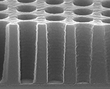
CEA-Leti achieves 400°C CMOS fabrication milestone for 3D chip stacking
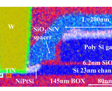
ChatGPT said: CEA-Leti announced it has built working 2.5-volt silicon-on-insulator CMOS chips at just 400°C. That is low enough to stack them atop finished circuitry without risking damage to the layers below, a hurdle that has long stalled progress toward denser, more efficient 3D chip designs. The French research institute, leading the EU’s FAMES pilot…
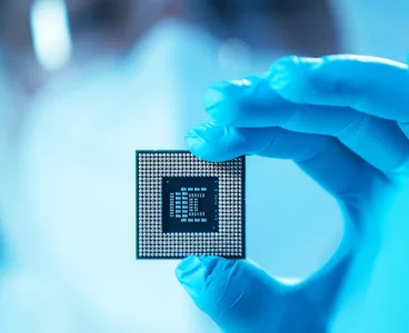
Materials driving the next phase in semiconductor performance
Exploring SiC, GaN and 2D materials in high-power and high-frequency applications For more than half a century, silicon has been the primary material in semiconductor technology. Its mature processing infrastructure and favorable electronic properties made it the default choice for most electronic devices. As demands for higher power density, faster switching and greater energy efficiency…
NVIDIA becomes major Intel CPU buyer in $5B collaboration
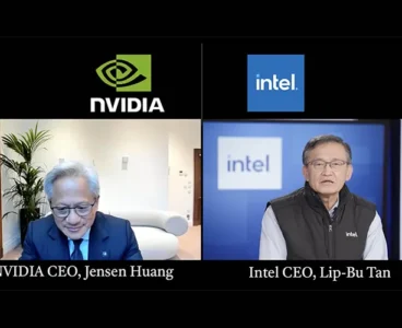
“The cognac was excellent; just not enough of it. I think [it] was from 1912,” Jensen Huang said on the livestream, moments before the press conference began. Intel’s Lip-Bu Tan answered, “Wow. 1912.” Those words would set the tone for what would be a reversal of fortunes. Decades ago, it would have seemed unthinkable that…
iPhone 17 Pro, rumored to add vapor-chamber cooling and a 48MP telephoto, is tracking a September launch

Apple hasn’t announced dates, but multiple outlets that track Cupertino’s annual cadence point to an iPhone 17 family reveal in the second week of September, with pre-orders that Friday and retail availability the Friday after. Based on Apple’s pattern and current reporting, the most plausible schedule is a keynote on Tuesday, September 9, 2025, pre-orders…
Reported Apple code leak points to new hardware roadmap with new chips, devices incoming

A new smart home hub. A revised Apple TV. A revamped Siri. Those are just some of the rumored products in Apple’s pipeline. The purported leak, which MacRumors revealed, suggests a significant push into the smart home and AI, domains where the Cupertino, California-based firm once innovated but has arguably fallen behind. Apple’s software code…
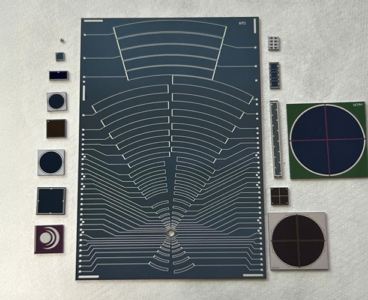
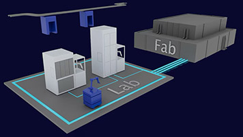
Bridging the lab-to-fab gap accelerates semiconductor innovation and commercialization

As the semiconductor industry evolves to meet surging demand for AI chips and advanced data infrastructure, its future will be defined not only by design ingenuity or scaling laws but by the breakthroughs happening at the molecular level. Materials science is emerging as the cornerstone of next-generation semiconductor innovation. The push for smaller, faster and…
The 2025 R&D 100 Finalists are here

A total of 158 Finalists for the 2025 R&D 100 Awards have been announced by R&D World. Now in its 63rd year, this renowned global science and innovation competition drew entries from 13 countries/regions. This year’s esteemed judging panel featured 54 respected industry professionals from across the globe. The Finalists are listed below by category,…
Trump tags Intel CEO as ‘conflicted’ and wants him gone

Intel Corp.’s board barely had time to hand Lip-Bu Tan the keys to the corner office before President Donald Trump grabbed a megaphone. On August 7, 2025, the president blasted Intel’s CEO as “highly conflicted” and called on the chipmaker’s newly installed leader to step down. Coming from a sitting U.S. president, the public rebuke…
Top 5 R&D moves this week: Intel’s chip retreat, antimatter breakthrough and AI’s metabolic twin steal the show

In this week’s R&D roundup, Lawrence Livermore National Laboratory lands a deal to construct a cutting-edge telescope for space surveillance, while researchers crack the 1918 flu virus genome. In tech, Intel mulls bowing out of the bleeding-edge chip battle as it continues to struggle to adapt in a quickly-evolving hardware landscape while NVIDIA sees a…
First MCU combines gigahertz CPU, 35× faster AI engine and MRAM in single device
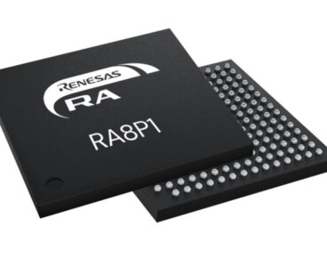
Japanese semiconductor firm Renesas Electronics has unveiled the RA8P1, positioning it as a breakthrough microcontroller that integrates gigahertz-class processing, dedicated AI acceleration hardware and magnetoresistive RAM (MRAM) on a single 22-nanometer chip. The chip includes graphics capabilities, multiple connectivity interfaces and advanced security features typically associated with higher-end processors. In a press briefing, Renesas billed…
Stargate’s $500B bet could force data-center and 1.2 GW grid rethink
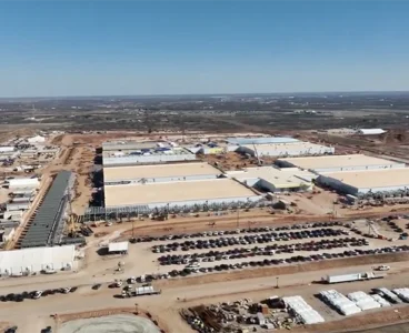
Crews in Abilene, Texas, are turning a 875-acre site of red clay into a data-center campus that will draw 1.2 GW, enough to conservatively support the load of 750,000 homes, once all eight “AI factory” halls are online, part of Stargate’s headline-grabbing $500 billion build-out. Bloomberg’s hard-hat tour captured Crusoe CEO Chase Lochmiller describing the project…
Compact AI model lets popular ESP32 microcontroller predict network failures and memory leaks in real time
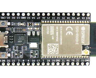
Santa Clara-based startup OTAinfo has introduced an on-device AI system designed to enhance reliability on Espressif’s popular and low-cost ESP32 microcontrollers. The embedded intelligence layer, which the company compared in a LinkedIn post to “ChatGPT for ESP32,” runs entirely within the device’s firmware using only 32 kb of memory to predict network communication failures and…
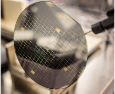
TSMC’s N3P hits mass production, with N3X customer sampling slated for Q3–Q4 2025a

TSMC has flipped the switch on its performance-tuned N3P process, bringing the 3-nm node into volume production after Q4 2024 pilot runs. Next up is the higher-voltage, speed-focused N3X variant, now slated to sample by Q3–Q4 2025. “N3P started production late last year, in 2024,” Kevin Zhang, TSMC’s deputy COO, told Tom’s Hardware at the…
7 major R&D developments this week: Tariff uncertainty persists, Pfizer sells campus, Scania acquires Northvolt unit
Uncertainty surrounding U.S. tariff policy impacted R&D sectors this week, even as the broader market showed gains. The R&D World Index (RDWI) for the week ending April 11, 2025, closed at 3,585.25, up 2.25% (or 78.98 basis points). Performance among the 25 RDWI member companies was mixed, with twelve gaining value. Leading the pack was…
While Trump tariffs spare phones/PCs, R&D could faces GPU cost pressures

President Trump’s recent tariff actions exempted key consumer electronics like smartphones and computers, and thus have shielded average consumers. Yet R&D groups that are planning on investing in GPUs for local inference face a potential cost shock, as graphics card imports are now subject to steep duties—reaching up to 145% if assembled in China. While…
Why IBM predicts quantum advantage within two years
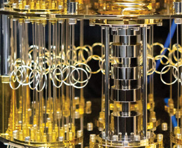
Industry analysts from McKinsey to Omdia largely converge on a timeline for initial quantum advantage emerging in the next few years. While the era when quantum computers can routinely tackle large-scale challenges in fields like drug discovery and materials science might still be years away, IBM’s Quantum CTO, Oliver Dial, Ph.D., predicts the threshold of…
How OMRON integrates virtual humans and factory expertise into NVIDIA Omniverse digital twins

Picture this: A GPU-accelerated CT X-ray inspection machine peering into circuit boards at 0.2 µm/pix resolution, paired with a virtual human assistant that explains, tweaks, and optimizes the process in plain language. That’s precisely what industrial automation giant OMRON showcased at NVIDIA’s GTC 2025 last week. At the heart of the demo was OMRON’s VT-X…
Thermo Fisher launches Vulcan Automated Lab to accelerate semiconductor analysis with AI-powered TEM metrology workflow
Thermo Fisher Scientific has unveiled the Vulcan Automated Lab, a fully integrated system designed to streamline transmission electron microscopy (TEM) workflows and enhance semiconductor process control. The industry is under increasing pressure to deliver atomic-scale precision at high volumes amid global demand for advanced chips. The Vulcan system integrates robotic sample handling, artificial intelligence (AI)-enhanced…
How could Lip-Bu Tan’ shake up Intel’s R&D priorities?

There’s a new sheriff in town at Intel, and his name is Lip-Bu Tan, a seasoned semiconductor veteran stepping into the CEO role. He will be charged with steering the beleaguered chipmaker back toward a more sustainable financial future. Tan, the former CEO of Cadence Design Systems and founder of venture capital firm Walden International,…