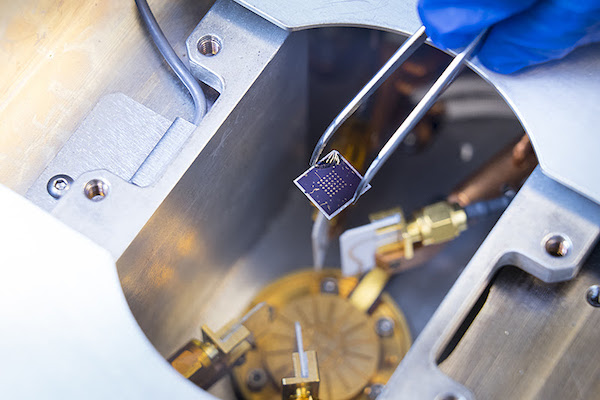
Researchers have created a more feasible way to combine transistors and memory on a chip, potentially bringing faster computing. (Purdue University photo/Vincent Walter)
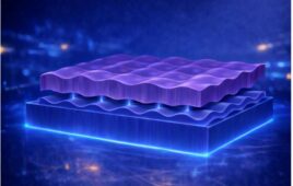
A computer chip processes and stores information using two different devices. If engineers could combine these devices into one or put them next to each other, then there would be more space on a chip, making it faster and more powerful.
Purdue University engineers have developed a way that the millions of tiny switches used to process information – called transistors – could also store that information as one device.
The method, detailed in a paper published in Nature Electronics, accomplishes this by solving another problem: combining a transistor with higher-performing memory technology than is used in most computers, called ferroelectric RAM.
Researchers have been trying for decades to integrate the two, but issues happen at the interface between a ferroelectric material and silicon, the semiconductor material that makes up transistors. Instead, ferroelectric RAM operates as a separate unit on-chip, limiting its potential to make computing much more efficient.
A team led by Peide Ye, the Richard J. and Mary Jo Schwartz Professor of Electrical and Computer Engineering at Purdue, discovered how to overcome the mortal enemy relationship between silicon and a ferroelectric material.
“We used a semiconductor that has ferroelectric properties. This way two materials become one material, and you don’t have to worry about the interface issues,” Ye said.
The result is a so-called ferroelectric semiconductor field-effect transistor, built in the same way as transistors currently used on computer chips.
The material, alpha indium selenide, not only has ferroelectric properties, but also addresses the issue of a conventional ferroelectric material usually acting as an insulator rather than a semiconductor due to a so-called wide “band gap,” which means that electricity cannot pass through and no computing happens.
Alpha indium selenide has a much smaller band gap, making it possible for the material to be a semiconductor without losing ferroelectric properties.
Mengwei Si, a Purdue postdoctoral researcher in electrical and computer engineering, built and tested the transistor, finding that its performance was comparable to existing ferroelectric field-effect transistors, and could exceed them with more optimization. Sumeet Gupta, a Purdue assistant professor of electrical and computer engineering, and Ph.D. candidate Atanu Saha provided modeling support.
Si and Ye’s team also worked with researchers at the Georgia Institute of Technology to build alpha indium selenide into a space on a chip, called a ferroelectric tunneling junction, which engineers could use to enhance a chip’s capabilities. The team presented this work at the 2019 IEEE International Electron Devices Meeting, held this week.
In the past, researchers hadn’t been able to build a high-performance ferroelectric tunneling junction because its wide band gap made the material too thick for electrical current to pass through. Since alpha indium selenide has a much smaller band gap, the material can be just 10 nanometers thick, allowing more current to flow through it.
More current allows a device area to scale down to several nanometers, making chips more dense and energy efficient, Ye said. A thinner material – even down to an atomic layer thick – also means that the electrodes on either side of a tunneling junction can be much smaller, which would be useful for building circuits that mimic networks in the human brain.
This research was performed in the Purdue Discovery Park Birck Nanotechnology Center and supported by the National Science Foundation, Air Force Office of Scientific Research, Semiconductor Research Corporation, Defense Advanced Research Projects Agency and the U.S. Office of Naval Research.
About Discovery Park
Discovery Park is a place where Purdue researchers move beyond traditional boundaries, collaborating across disciplines and with policymakers and business leaders to create solutions for a better world. Grand challenges of global health, global conflict and security, and those that lie at the nexus of sustainable energy, world food supply, water and the environment are the focus of researchers in Discovery Park. The translation of discovery to impact is integrated into the fabric of Discovery Park through entrepreneurship programs and partnerships.
Writer: Kayla Wiles, 765-494-2432, [email protected]