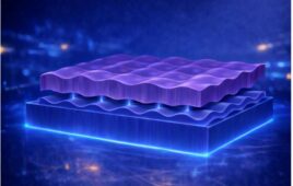
 To say that the chips powering the current AI wave are hot is an understatement. NVIDIA booked $39.1 billion in data center revenue in the first quarter of fiscal 2026, a 73% bump year over year. But they are, of course, also hot physically. The B200, a flagship Blackwell GPU, draws up to 1,000 watts. When NVIDIA started stacking 72 of them into a single rack, early customers including Microsoft, Google, and Meta ran into overheating problems and connectivity glitches. The heat challenge extends across the ecosystem. Direct-to-chip liquid cooling is becoming the default for the highest-density AI racks and training clusters. AMD’s Instinct MI355X draws up to 1,400 watts per accelerator and is aimed largely at liquid-cooled deployments. Google builds its Ironwood TPU superpods around 9,216 liquid-cooled chips.
Marco Provolo is not surprised by the cooling focus. The heat problem has been a concern for years, he said in a recent interview, and “with AI it’s just getting worse.” He continued: “We’re going very close to the theoretical limit where you’re not able to pull heat out anymore, because there’s a physical limit to the quantity of heat per square centimeter that you can extract.”
Electrical interconnects consume more power than optical links, and that power draw rises with bandwidth and distance. That is one reason so many components are packed tightly onto a single board today. “When you start moving things apart, the consumption booms,” Provolo said. “That’s basically why you have everything on a single board today. When you start moving things apart, that’s where heating problems start.”
Provolo is an executive manager and head of connected ecosystem at NTT DATA Italia. IOWN, the Innovative Optical and Wireless Network, is NTT’s long-running R&D initiative.
Even as AI infrastructure costs remain under pressure from tight supply and rising memory and server-component prices, Provolo argues the deeper constraint is still data movement and heat. That pressure, developed through NTT’s IOWN initiative, is what he thinks will shape the next decade of AI infrastructure. His argument: the industry has been trying to solve yesterday’s problem. The constraint on scaling is how much data you can move, how far, and how much heat you are willing to concentrate in one building to do it.
The conversation below, from an interview at NTT Upgrade 2026, has been edited for length and clarity
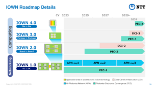
An IOWN roadmap from NTT
Buntz: The field of photonics is getting traction. NVIDIA, AMD and Intel all are focusing on photonics now. What’s your take given NTT’s historical focus on the area?
Marco Provolo
Provolo: Yes, though there’s still copper everywhere, just because it’s working. In my opinion, they’re going to face problems with consumption when you have 500 kilowatts per rack. [Editorial note: NVIDIA’s Kyber/Rubin Ultra racks, for instance, are publicly targeted beyond that range — at 600 kW in 2027.]
That’s part of why we created a consortium. It’s not a single-player solution. It comes from research, and it applies in many different contexts.
What we’ve been working on is the ability to play around with light on silicon, using the same production systems you use today, but with the ability to handle light. What you need is the ability to convert between electricity and light. This has been done in the past. The remote control of a television is basically the same thing: you send light, you receive light. The challenge here was 500-gigabit bandwidth in a tiny device. That happened, and it’s been commercial since 2022. The device is called a transceiver.
| Metrics group | Phase 1 (2024) | Phase 2 (2027) | Phase 3 (by 2030) |
|---|---|---|---|
| Logical node composability |
|
|
|
| Data movement space/cost |
|
|
|
| Deterministic | Limited to nondeterministic | ms-level deterministic | 10s us-level deterministic |
| Energy/cost efficiency | Independent from workloads/events/traffic | Closely match with workloads/events/traffic | Strive for order-of-magnitude reduction as compared to Phase 2 |
| Security | Classic (e.g., by RSA, DH) | Post-quantum security for data in use and at rest |
|
| Credit: IOWN Global Forum, KVaTE Roadmap 2.0 | |||
Buntz: Can you walk me through IOWN’s roadmap and what the current status looks like?
Provolo: We talk about APN, or All-Photonics Network. That’s the network concept behind it. The problem with today’s networks, especially telco networks, is that you don’t have a full photonic path. Conversion from photonics to electronics means packet loss, higher jitter, retransmission and loss in bandwidth and speed.
And just to be clear, this isn’t our IP alone. We’ve built an ecosystem around IOWN and Open APN that includes collaborators such as Ciena, Fujitsu, NEC and Nokia.
Buntz: So there are four stages in the roadmap, each pushing photonics closer to the silicon. PEC-1 is the networking/inter-datacenter stage. PEC-2 replaces electrical wiring between computer boards with optical links. PEC-3 sits between packages or neighboring chips. PEC-4 goes inside the chip itself. Where are you now, and what’s next?
| Generation | Area of application | Status |
|---|---|---|
| PEC-1 | Optical interconnect between data centers | Commercialized through APN |
| PEC-2 | Optical interconnect between boards in computing equipment | Commercialization targeted in 2026 |
| PEC-3 | Optical interconnect between chips on the same board | In development |
| PEC-4 | Optical wiring within individual chips | In development |
| Source: NTT DATA | ||
Provolo: We finished deploying PEC-1, with Open APN collaborators including Ciena, Fujitsu, NEC and Nokia. PEC-2 is about inter-board interconnection. PEC-3 is a little further down the road, and so is PEC-4. We have samples of PEC-3 in Tokyo, and we’re working on making it ready for production. That’s intra-board connection: instead of copper wires on the board, you have a photonic connection at the chip level. So a provocative thought: do you need a board tomorrow? If you’re able to connect with optical fiber, the concept of a board somehow disappears.
PEC-4 is intra-chip, between the silicon dies inside the chip. Just to clarify, this is not photonic computing, which uses light to get computational results. This is about communication.
What we expect is that you stop thinking about edge cloud, remote cloud, closed data center, edge data center and micro data center. Over 300 kilometers you get one millisecond of latency. Sometimes you want to be faster than that. It’s a theoretical limit for the physics we know, and you can’t overcome it. What we offer is the best network possible, because we’re not converting from light to electricity and back at many points along the path.
Buntz: What parallels do you see with the dot-com bubble and the fiber optic investment back then?
Provolo: One effect leads to AI. Because you need to move data here and there, the boom of AI leads to a boom of networking. You need infrastructure. You cannot use the same infrastructure you had before.
There are a couple of different problems. One is models and the resources they require. We’re working on that too. Tsuzumi is one big thing we’ve been developing over the last couple of years, a small language model that can run on the edge, and “edge” might mean this computer or even a single GPU. That’s a little outside the scope of what I’m talking about now.
But if you need a model with a lot of your company data, and you need to make it work, there will be some efficiency concepts that need to enter the equation. It’s not possible that every employee tomorrow will have thousands of agents running on their job.