Capturing and manipulating light at nanoscale is a key factor to build high efficiency solar cells. Researchers in the 3D Photovoltaics group have recently presented a promising new design. Their simulations show that vertically stacked nanowires on top of ultrathin silicon films reduces the total amount of material needed by 90 percent while increasing the…
Researchers Uncover Rare New Layered Ferromagnetic Semiconductor
Collaborating scientists at the U.S. Department of Energy’s Ames Laboratory, Brookhaven National Laboratory, and Princeton University have discovered a new layered ferromagnetic semiconductor, a rare type of material that holds great promise for next-generation electronic technologies. As the name implies, semiconductors are the Goldilocks of electrically conductive materials—not a metal, and not an insulator, but…
Next-gen Logic Devices Result from Photodoping in 2-D Materials
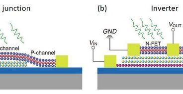
National University of Singapore scientists have discovered a method for photoinduced electron doping on molybdenum ditelluride (MoTe2) heterostructures for fabricating next generation logic devices. Two-dimensional (2-D) transition metal dichalcogenides (TMDs) are promising building blocks for the development of next generation electronic devices. These materials are atomically thin and exhibit unique electrical properties. Researchers are interested…
Integrated Sensors for Direct Control
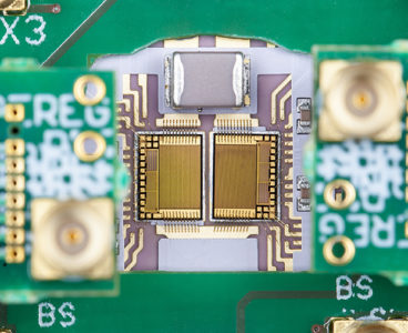
A team of Fraunhofer researchers has succeeded in significantly enhancing the functionality of GaN power ICs for voltage converters: the researchers at Fraunhofer IAF integrated current and temperature sensors onto a GaN-based semiconductor chip, along with power transistors, freewheeling diodes and gate drivers. This development paves the way for more compact and efficient on-board chargers…
Semiconductor Scientists Uncover ‘Impossible’ Effect
A physical effect known as superinjection underlies modern light-emitting diodes (LEDs) and lasers. For decades this effect was believed to occur only in semiconductor heterostructures—that is, structures composed of two or more semiconductor materials. Researchers from the Moscow Institute of Physics and Technology have found superinjection to be possible in homostructures, which are made of…
ON Semiconductor to Acquire, Preserve GLOBALFOUNDRIES Fab Plant
Governor Andrew M. Cuomo has announced that ON Semiconductor, a Fortune 500 company with a global customer base, will expand operations in New York State by purchasing and preserving the existing GLOBALFOUNDRIES Fab 10 manufacturing facility located in East Fishkill, Dutchess County. ON Semiconductor has committed to invest more than $720 million over 10 years…
Light Produced from Exotic Particle States
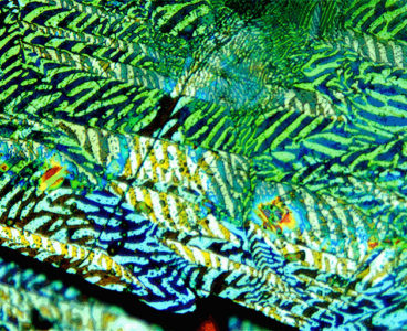
A new type of light-emitting diode has been developed at TU Wien. Light is produced from the radiative decay of exciton complexes in layers of just a few atoms thickness. When particles bond in free space, they normally create atoms or molecules. However, much more exotic bonding states can be produced inside solid objects. Researchers…
Measurement of Semiconductor Material Quality Has Gotten 100,000 Times More Sensitive
The enhanced power of the new measuring technique to characterize materials at scales much smaller than any current technologies will accelerate the discovery and investigation of 2D, micro- and nanoscale materials. Being able to accurately measure semiconductor properties of materials in small volumes helps engineers determine the range of applications for which these materials may…
Almost Perfect Performance Recorded in Low-cost Semiconductors
Tiny, easy-to-produce particles, called quantum dots, may soon take the place of more expensive single crystal semiconductors in advanced electronics found in solar panels, camera sensors and medical imaging tools. Although quantum dots have begun to break into the consumer market—in the form of quantum dot TVs—they have been hampered by long-standing uncertainties about their…
A New Way to Control Light from Hybrid Crystals
Scientists have found a new way to control light emitted by exotic crystal semiconductors, which could lead to more efficient solar cells and other advances in electronics, according to a Rutgers-led study in the journal Materials Today. Their discovery involves crystals called hybrid perovskites, which consist of interlocking organic and inorganic materials, and they have…
Quantum Sensor Improves Cancer Treatment, Long-range 3D Imaging
A new quantum sensor developed by researchers at the University of Waterloo’s Institute for Quantum Computing (IQC) has proven it can outperform existing technologies and promises significant advancements in long-range 3D imaging and monitoring the success of cancer treatments. The sensors are the first of their kind and are based on semiconductor nanowires that can…
New Technique Synthesizes Nanographene on Metal Oxide Surfaces
Nanostructures based on carbon are promising materials for nanoelectronics. However, to be suitable, they would often need to be formed on non-metallic surfaces, which has been a challenge—up to now. Researchers at Friedrich-Alexander-Universitäthave found a method of forming nanographenes on metal oxide surfaces. Their research, conducted within the framework of collaborative research centre 953—Synthetic Carbon…
Repulsive Photons Avoid Each Other in Semiconductor Material
Light particles normally do not “feel” each other because there is no interaction acting between them. Researchers at ETH have now succeeded in manipulating photons inside a semiconductor material in such a way as to make them repel each other nevertheless. Two light beams crossing each other do not deflect one another. That is because,…
Room Temperature, 2D Platform Advances Quantum Technology
Quantum computers promise to be a revolutionary technology because their elementary building blocks, qubits, can hold more information than the binary, 0-or-1 bits of classical computers. But to harness this capability, hardware must be developed that can access, measure and manipulate individual quantum states. Researchers at the University of Pennsylvania’s School of Engineering and Applied…
Physicists Create Revolutionary Exotic Electron Liquid
By bombarding an ultrathin semiconductor sandwich with powerful laser pulses, physicists at the University of California, Riverside, have created the first “electron liquid” at room temperature. The achievement opens a pathway for development of the first practical and efficient devices to generate and detect light at terahertz wavelengths—between infrared light and microwaves. Such devices could…
Visible Laser to Study Semiconductor Properties
LED lights and monitors, and quality solar panels were born of a revolution in semiconductors that efficiently convert energy to light or vice versa. Now, next-generation semiconducting materials are on the horizon, and in a new study, researchers have uncovered eccentric physics behind their potential to transform lighting technology and photovoltaics yet again. Comparing the…
Breakthrough Could Double Efficiency of Organic Electronics
Researchers from Chalmers University of Technology in Sweden have discovered a simple new tweak that could double the efficiency of organic electronics. OLED-displays, plastic-based solar cells and bioelectronics are just some of the technologies that could benefit from their new discovery, which deals with “double-doped” polymers. The majority of our everyday electronics are based on…
Interatomic Light Rectifier Generates Directed Electric Currents
The absorption of light in semiconductor crystals without inversion symmetry can generate electric currents. Researchers at the Max-Born-Institute have now generated directed currents at terahertz (THz) frequencies, much higher than the clock rates of current electronics. They show that electronic charge transfer between neighboring atoms in the crystal lattice represents the underlying mechanism. Solar cells…
Scientists Push Quantum Optic Networks Closer to Reality
Scientists have moved quantum optic networks a step closer to reality. The ability to precisely control the interactions of light and matter at the nanoscale could help such a network transmit larger amounts of data more quickly and securely than an electrical network. A team of researchers at the U.S. Department of Energy’s (DOE) Argonne…
Two Dimensions Are Better than Three
For the past 60 years, the electronics industry and the average consumer have benefited from the continuous miniaturization, increased storage capacity and decreased power consumption of electronic devices. However, this era of scaling that has benefited humanity is rapidly coming to end. To continue shrinking the size and power consumption of electronics, new materials and…
New Quantum Materials Could Take Computing Devices Beyond the Semiconductor Era
Researchers from Intel Corp. and the University of California, Berkeley, are looking beyond current transistor technology and preparing the way for a new type of memory and logic circuit that could someday be in every computer on the planet. In a paper appearing online Dec. 3 in advance of publication in the journal Nature, the…
Faster Electrons Improve Semiconductors
Researchers have found a way to speed up the electrons in semiconductors, which could lead to improved solar power and transistor use. A team from the Graduate School of Bio-Applications and Systems Engineering at the Tokyo University of Agriculture and Technology (TUAT) have found a process to speed up the movement of electrons in organic…
Hidden Gapless States on the Path to Semiconductor Nanocrystals
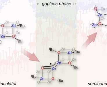
When chemists from the Institute of Physical Chemistry of the Polish Academy of Sciences in Warsaw were starting work on a new material designed for the efficient production of nanocrystalline zinc oxide, they didn’t expect any surprises. They were thus greatly astonished when the electrical properties of the changing material turned out to be extremely…
New Electrochemistry Theory Decodes Unexplained Behavior
When it comes to designing and optimizing mechanical systems, scientists understand the physical laws surrounding them well enough to create computer models that can predict their properties and behavior. However, scientists who are working to design better electrochemical systems, such as batteries or supercapacitors, don’t yet have a comprehensive model of the driving forces that…
Boron Nitride Separation Process Could Facilitate Higher Efficiency Solar Cells
A team of semiconductor researchers based in France has used a boron nitride separation layer to grow indium gallium nitride (InGaN) solar cells that were then lifted off their original sapphire substrate and placed onto a glass substrate. By combining the InGaN cells with photovoltaic (PV) cells made from materials such as silicon or gallium…


