Research & Development World

  • R&D World Home
  • Topics
    • Aerospace
    • Automotive
    • Biotech
    • Careers
    • Chemistry
    • Environment
    • Energy
    • Life Science
    • Material Science
    • R&D Management
    • Physics
  • Technology
    • 3D Printing
    • A.I./Robotics
    • Software
    • Battery Technology
    • Controlled Environments
      • Cleanrooms
      • Graphene
      • Lasers
      • Regulations/Standards
      • Sensors
    • Imaging
    • Nanotechnology
    • Scientific Computing
      • Big Data
      • HPC/Supercomputing
      • Informatics
      • Security
    • Semiconductors
  • R&D Market Pulse
  • R&D 100
    • 2025 R&D 100 Award Winners
    • 2025 Professional Award Winners
    • 2025 Special Recognition Winners
    • R&D 100 Awards Event
    • R&D 100 Submissions
    • Winner Archive
  • Resources
    • Research Reports
    • Digital Issues
    • Educational Assets
    • Subscribe
    • Video
    • Webinars
    • Content submission guidelines for R&D World
  • Global Funding Forecast
  • Top Labs
  • Advertise
  • SUBSCRIBE

ACM Research’s new facility contributes to PNW’s growing semiconductor industry  

By Heather Hall | November 26, 2023

ACM 
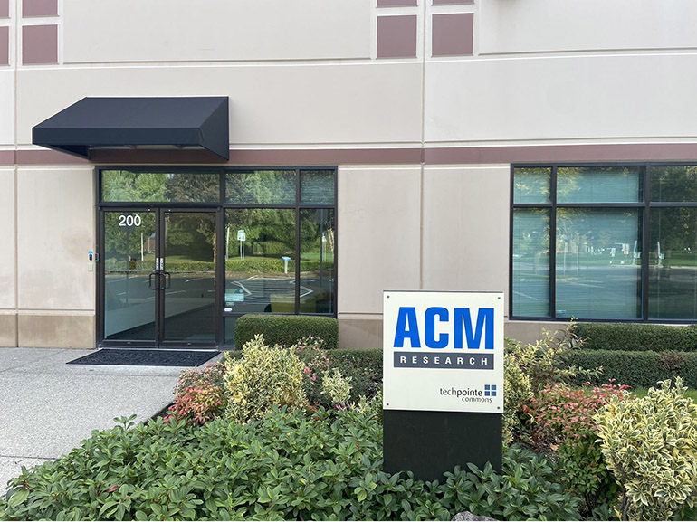
Research, a supplier of wafer processing solutions for semiconductor and advanced wafer-level packaging (WLP) applications, announces the grand opening of its new multi-use facility in Hillsboro, Oregon, on November 28. This is a first-of-its-kind property within North America for ACM Research, and its 11,000 ft2 will feature offices, warehouse space, and a dedicated cleanroom/demonstration lab.

“Our company sits at a rapid growth juncture as everyone from high-volume manufacturers to logistics providers are restructuring how they do business. Our expertise lies in delivering tailored solutions that cater to the unique requirements of innovation-driven businesses. We have a proven track record of successfully supporting companies in their quest for breakthroughs and advancements and see limitless potential to leverage our expertise in North America and globally,” said Jim Straus, vice president of sales for the U.S. and Europe.

The Hillsboro facility is strategically located near key customers and partners and will serve as the new sales and service hub for ACM Research. With the construction of the new building, the company anticipates doubling its number of U.S. employees to support current and potential customers.

With the development of the cleanroom and demonstration space, ACM Research can grow its North American footprint and present a showcase space where current and future customers have the hands-on opportunity to evaluate and test new tools. With the ability to demonstrate its customizable and agile solutions, ACM Research will facilitate access to essential semiconductor infrastructure and resources to drive innovation and enhance local talent development.

“Known as the ‘Silicon Forest,’ the Pacific Northwest, and Hillsboro in particular, continues to be a growing semiconductor manufacturing hub, spurring innovation and creating jobs. This is another step in the chip industry’s progress toward becoming a trillion-dollar industry,” said Straus.


Related Articles Read More >

Trump administration abandons Supreme Court challenge to NIH indirect cost cap
U.S. and Korea solidify AI-energy pact: Genesis Mission and K-Moonshot join forces
Machine learning rewrites the rules for measuring scientific disruption
Billionaires, chip makers and one physicist: inside Trump’s PCAST picks
rd newsletter
EXPAND YOUR KNOWLEDGE AND STAY CONNECTED
Get the latest info on technologies, trends, and strategies in Research & Development.

R&D World Digital Issues

Fall 2025 issue

Browse the most current issue of R&D World and back issues in an easy to use high quality format. Clip, share and download with the leading R&D magazine today.

R&D 100 Awards
Research & Development World
  • Subscribe to R&D World Magazine
  • Sign up for R&D World’s newsletter
  • Contact Us
  • About Us
  • Drug Discovery & Development
  • Pharmaceutical Processing
  • Global Funding Forecast

Copyright © 2026 WTWH Media LLC. All Rights Reserved. The material on this site may not be reproduced, distributed, transmitted, cached or otherwise used, except with the prior written permission of WTWH Media
Privacy Policy | Advertising | About Us

Search R&D World

  • R&D World Home
  • Topics
    • Aerospace
    • Automotive
    • Biotech
    • Careers
    • Chemistry
    • Environment
    • Energy
    • Life Science
    • Material Science
    • R&D Management
    • Physics
  • Technology
    • 3D Printing
    • A.I./Robotics
    • Software
    • Battery Technology
    • Controlled Environments
      • Cleanrooms
      • Graphene
      • Lasers
      • Regulations/Standards
      • Sensors
    • Imaging
    • Nanotechnology
    • Scientific Computing
      • Big Data
      • HPC/Supercomputing
      • Informatics
      • Security
    • Semiconductors
  • R&D Market Pulse
  • R&D 100
    • 2025 R&D 100 Award Winners
    • 2025 Professional Award Winners
    • 2025 Special Recognition Winners
    • R&D 100 Awards Event
    • R&D 100 Submissions
    • Winner Archive
  • Resources
    • Research Reports
    • Digital Issues
    • Educational Assets
    • Subscribe
    • Video
    • Webinars
    • Content submission guidelines for R&D World
  • Global Funding Forecast
  • Top Labs
  • Advertise
  • SUBSCRIBE