ChatGPT said:
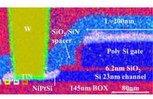 CEA-Leti announced it has built working 2.5-volt silicon-on-insulator CMOS chips at just 400°C. That is low enough to stack them atop finished circuitry without risking damage to the layers below, a hurdle that has long stalled progress toward denser, more efficient 3D chip designs.
The French research institute, leading the EU’s FAMES pilot line, said the low-heat devices deliver electrical performance on par with those made at conventional temperatures over 1,000°C. The work, detailed in a paper at the International Electron Devices Meeting in San Francisco, relies on techniques like nanosecond laser annealing to activate dopants and regrow silicon, paving the way for multi-tier chips that blend logic with RF or sensor functions under the EU Chips Act’s push for semiconductor independence.
According to the team, the 400 °C flow supports stacking CMOS layers above finished circuitry without exceeding thermal limits that could degrade underlying devices. The approach is aimed at multi-tier systems combining logic with functions such as RF, smart pixels, or power management.
FAMES, launched in 2023 under the EU Chips Act strategy, is focused on FD-SOI platforms and more-than-Moore applications. The consortium includes CEA-Leti and partners such as imec, Fraunhofer, VTT, CEZAMAT WUT, Tyndall, Silicon Austria Labs, several universities, and other European research institutes.
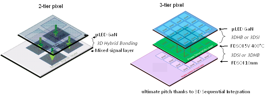
Concept for a three-tier micro-LED GaN pixel that enables a dense emissive array with reduced pitch, using 3D sequential integration (3DSI) and 3D hybrid bonding. CEA-Leti’s 400°C CMOS process supports top-tier integration without exceeding thermal limits for the active circuitry below.