
A research team at Sandia National Laboratories has successfully used machine learning — computer algorithms that improve themselves by learning patterns in data — to complete cumbersome materials science calculations more than 40,000 times faster than normal. Their results, published Jan. 4 in npj Computational Materials, could herald a dramatic acceleration in the creation of…
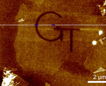
ORNL’s groundbreaking experiment tracks real-time transport of individual molecules

The animation depicts the controlled transport of a single molecule between two scanning tunneling microscope tips in an experiment at ORNL. Credit: Michelle Lehman/ORNL, U.S. Dept. of Energy Oak Ridge National Laboratory’s Center for Nanophase Materials Sciences, or CNMS, contributed to a groundbreaking experiment published in Science that tracks the real-time transport of individual molecules.…
What is graphene?

Graphene is a flat hexagonal lattice of carbon atoms, just one atom thick. It is a form of carbon related to carbon nanotubes and buckyballs (C60). Although it has always occurred naturally, it is only recently that it has been isolated and it’s individual properties examined. It is now known that graphene has exceptional electrical,…
Park Systems announces NanoScientific Symposium Asia, Nov. 24-25, 2020

Park Systems and NanoScientific Publications announce NanoScientific Symposium Asia, which will be held virtually, Nov. 24-25, 2020. The event will help nanoscience researchers and scientists catch up on the latest studies being formed using SPM and is sponsored by Physics World and Nanotechnology World Association. “NanoScientific Symposium Asia is a valuable opportunity for people doing…
E-beam atomic-scale 3-D ‘sculpting’ could enable new quantum nanodevices
By varying the energy and dose of tightly focused electron beams, researchers have demonstrated the ability to both etch away and deposit high-resolution nanoscale patterns on two-dimensional layers of graphene oxide. The 3D additive/subtractive “sculpting” can be done without changing the chemistry of the electron beam deposition chamber, providing the foundation for building a new…
Purdue 2-dimensional nanomaterial shows promise for high-speed electronics, quantum devices and defense tools
By Chris Adam Purdue University researchers have passed another significant milestone as they work to take a new two-dimensional nanomaterial to market for use in nanoelectronics, quantum devices and infrared technology used in national defense tools and biochemical sensors. The Purdue team received a U.S. patent for the nanomaterial, derived from the rare element tellurium,…
Microscopic robots ‘walk’ thanks to laser tech

by Cornell University A Cornell University-led collaboration has created the first microscopic robots that incorporate semiconductor components, allowing them to be controlled – and made to walk – with standard electronic signals. These robots, roughly the size of paramecium, provide a template for building even more complex versions that utilize silicon-based intelligence, can be mass…
Creating the best TV screen yet: Breakthrough in blue quantum dot technology

There are many things quantum dots could do, but the most obvious place they could change our lives is to make the colors on our TVs and screens more pristine. Research using the Canadian Light Source (CLS) at the University of Saskatchewan is helping to bring this technology closer to our living rooms. Quantum dots…
EnergyX announces partnership with ProfMOF, leading Nanotechnology Innovation Lab
Energy Exploration Technologies (EnergyX) and ProfMOF announce a partnership between their companies to promote the use of Metal Organic Frameworks (MOFs), a relatively new class of nanotechnology materials suitable in the development of projects involving renewable energy and large-scale lithium-ion production and battery storage. ProfMOF is the world leader in the research and development of…
Argonne and Sentient Science develop game-changing computer modeling program to improve discovery and design of new materials

Researchers at the U.S. Department of Energy’s (DOE) Argonne National Laboratory, in conjunction with industry partner Sentient Science, are making the discovery and design of new materials — a notoriously time-consuming and costly process — significantly easier through the development of an artificial intelligence-based computer modeling framework. The research was awarded $150,000 through the DOE’s…
Fluorescent peptide nanoparticles in every color of the rainbow

The discovery of green fluorescent protein (GFP), which is made by a jellyfish, transformed cell biology. It allowed scientists to stitch the GFP sequence to proteins from other organisms to trace their movements and interactions in living cells. Now, researchers reporting in ACS Applied Materials & Interfaces have designed peptide nanoparticles that can each glow…
Nanomaterial gives robots chameleon skin

By Jules Bernstein A new film made of gold nanoparticles changes color in response to any type of movement. Its unprecedented qualities could allow robots to mimic chameleons and octopi — among other futuristic applications. Unlike other materials that try to emulate nature’s color changers, this one can respond to any type of movement, like…
New technique for polymer manufacturing with reduced solvents aimed at vehicle, packaging production

By Chris Adam A team of Purdue University innovators has developed a new way for manufacturers to use nanocellulose – a green nanomaterial derived from natural sources such as plant matter, for use in vehicles, food packaging and other manufactured items. Normally to process nanocellulose, solvents or other dispersants are usually added to the mixture…
Engineers put tens of thousands of artificial brain synapses on a single chip
Written by Jennifer Chu, MIT News Office MIT engineers have designed a “brain-on-a-chip,” smaller than a piece of confetti, that is made from tens of thousands of artificial brain synapses known as memristors — silicon-based components that mimic the information-transmitting synapses in the human brain. The researchers borrowed from principles of metallurgy to fabricate each…
What you need to know about the rapidly evolving nanoscience landscape

By Brian W. Anthony Nanotechnology continues to make headlines as use cases increase across a variety of industry sectors, ranging from medicine and homeland security to transportation, food and retail. But when it comes right down to it, the nanoscale is nothing more than a dimension; it’s just really, really small. Is it the size…
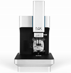
New system configurator for inverted microscopes & XY motorized stages, what to use when

To answer the demand for an integrated inverted microscope-positioning system that must match perfectly, PI (Physik Instrumente), a leader in precision motion control and nanopositioning solutions, has released an interactive brochure to aid in building the system by beginning with a fine positioner and/or a sample holder. Stages with piezo nanopositioning are incorporated to satisfy…
Ultra-Low Vibration Lab facilitates nanoengineering discoveries

By Steve Varma, Operations Manager, Minus K Technology The Ultra-Low Vibration Lab is a part of the new Center of Excellence in Nano Mechanical Science and Engineering (NAMSE) – a recent addition to the G.G. Brown Laboratories on the North Campus of the University of Michigan in Ann Arbor. Noel Perkins, former associate chair for…
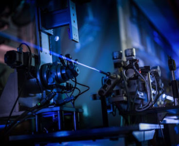
Scientists capture 3D images of nanoparticles, atom by atom, with unprecedented precision

Since their invention in the 1930s, electron microscopes have helped scientists peer into the atomic structure of ordinary materials like steel, and even exotic graphene. But despite these advances, such imaging techniques cannot precisely map out the 3D atomic structure of materials in a liquid solution, such as a catalyst in a hydrogen fuel cell,…
Park Systems Announces $1 million dollar Nano Research Grant Fund for researchers setting up nanoscience labs in North America
Park Systems, manufacturer of Atomic Force Microscopes, announces a $1 Million Dollar Nano Research Grant Fund to support researchers who are starting new nanoscience labs in North America. The Park Systems Nano Research Grant Fund provides up to twenty grants of $50,000 towards the purchase of any AFM system and accessories manufactured by Park Systems.…
Tough, flexible sensor invented for wearable tech
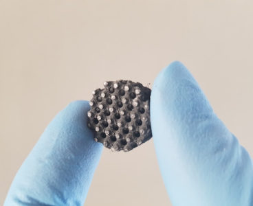
Researchers have utilized 3D printing and nanotechnology to create a durable, flexible sensor for wearable devices to monitor everything from vital signs to athletic performance. The new technology, developed by engineers at the University of Waterloo, combines silicone rubber with ultra-thin layers of graphene in a material ideal for making wristbands or insoles in running…
DNA-like material could bring even smaller transistors
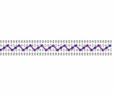
Computer chips use billions of tiny switches, called transistors, to process information. The more transistors on a chip, the faster the computer. A material shaped like a one-dimensional DNA helix might further push the limits on a transistor’s size. The material comes from a rare earth element called tellurium. Researchers found that the material,…
Universidad Politécnica de Madrid’s latest Magerit-3 supercomputer energizes and enables discovery in nuclear and material physics
By Ken Strandberg The European X-ray Free-electron Laser (European XFEL), recently completed its first experiments that captured images of an antibiotic-disabling enzyme. Scientists use X-rays to bombard molecules and project molecular smatterings on a sensor that reconstructs what the target looks like. With these high-energy X-rays we now have 3D visualizations of actual molecules, like…
Body heat through flexible fabric could power IoT devices for health monitoring for people, pets, machinery
Researchers at Purdue University have created a technology to address the thickness issue for wearable power generation. They developed a woven, thermoelectric, flexible fabric that is potentially thinner than a millimeter. “This wearable power generator is well-suited for body or other heat recovery while also offering great mechanical flexibility and comfort,” said Kazuaki Yazawa, a…
New material points toward highly efficient solar cells

A new type of material for next-generation solar cells eliminates the need to use lead, which has been a major roadblock for this technology. Solar cells, incorporating the mineral perovskite, have been the focus of attention since the material was first shown to work in 2009. Solar cells that are built using this material are…
Using Nanoparticles to Remove Micro-Contaminants From Water

There may be a new way to efficiently remove micro-contaminants from water. Researchers from ETH Zurich have created a new approach to removing chemical substances from water using multiferroic nanoparticles that induce the decomposition of chemical residues in contaminated water. A variety of chemical substances including cosmetics, medications, contraceptive pills, plant fertilizers and detergents are…