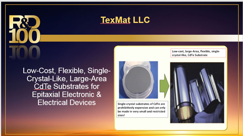
Low-Cost, Flexible, Single-Crystal-Like, Large-Area CdTe Substrates for Epitaxial Electronic & Electrical Devices provides a template for subsequent growth of electrical and electronic devices. Compared to CdTe single crystals that are more expensive and can be fabricated in very small sizes, these substrates are essentially transformational. Devices based on CdTe have numerous applications such as infrared detectors for applications from military night vision to deep space infrared telescopy; radiation detectors for X-ray and Y-ray detection for applications such as medical imaging, security monitoring, nuclear safeguarding and astrophysics; and it is best known for its application to photovoltaic devices. This product can be made in wide areas such as a meter wide and can also be fabricated in a roll-to-roll configuration. If such a low-cost, flexible, single-crystal-like substrate is used to grown heteroepitaxial devices, it will allow for fabrication of low-cost, large-area, flexible, high-performance CdTe-based devices such as photodetectors for short, medium and long wavelength IR radiation operating without cryogenic cooling.
Each year for more than 50 years, R&D Magazine has honored the 100 best innovations in research and development. We are currently accepting applications for the 2017 R&D 100 Awards. Innovators with an exceptional product developed between January 1, 2016 and March 31, 2017 should apply. Submissions close May 12, 2017.
For information on the 55th Annual R&D 100 Awards visit the R&D 100 Conference website.


