Research & Development World

  • R&D World Home
  • Topics
    • Aerospace
    • Automotive
    • Biotech
    • Careers
    • Chemistry
    • Environment
    • Energy
    • Life Science
    • Material Science
    • R&D Management
    • Physics
  • Technology
    • 3D Printing
    • A.I./Robotics
    • Software
    • Battery Technology
    • Controlled Environments
      • Cleanrooms
      • Graphene
      • Lasers
      • Regulations/Standards
      • Sensors
    • Imaging
    • Nanotechnology
    • Scientific Computing
      • Big Data
      • HPC/Supercomputing
      • Informatics
      • Security
    • Semiconductors
  • R&D Market Pulse
  • R&D 100
    • 2025 R&D 100 Award Winners
    • 2025 Professional Award Winners
    • 2025 Special Recognition Winners
    • R&D 100 Awards Event
    • R&D 100 Submissions
    • Winner Archive
  • Resources
    • Research Reports
    • Digital Issues
    • Educational Assets
    • Subscribe
    • Video
    • Webinars
    • PharmSci360
    • Content submission guidelines for R&D World
  • Global Funding Forecast
  • Top Labs
  • Advertise
  • SUBSCRIBE

Graphene Nanoribbons Produced on Large Scale for Electronics

By Lund University | January 23, 2019

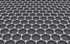
Two-dimensional sheets of graphene in the form of ribbons a few tens of nanometers across have unique properties that are highly interesting for use in future electronics. Researchers have now for the first time fully characterized nanoribbons grown in both the two possible configurations on the same wafer with a clear route towards upscaling the production.

Graphene in the form of nanoribbons show so called ballistic transport, which means that the material does not heat up when a current flow through it. This opens up an interesting path towards high speed, low power nanoelectronics. The nanoribbon form may also let graphene behave more like a semiconductor, which is the type of material found in transistors and diodes. The properties of graphene nanoribbons are closely related to the precise structure of the edges of the ribbon.

Also, the symmetry of the graphene structure lets the edges take two different configurations, so called zigzag and armchair, depending on the direction of the long respective short edge of the ribbon.

The nanoribbons were grown on a template made of silicon carbide under well controlled conditions and thoroughly characterized by a research team from MAX IV Laboratory, Techniche Universität Chemnitz, Leibniz Universität Hannover, and Linköping University. The template has ridges running in two different crystallographic directions to let both the armchair and zig-zag varieties of graphene nanoribbons form. The result is a predictable growth of high-quality graphene nanoribbons which have a homogeneity over a millimeter scale and a well-controlled edge structure.

One of the new findings is that the researchers were able to show ballistic transport in the bulk of the nanoribbon. This was possible due to extremely challenging four probe experiments performed at a length scale below 100 nm by the group in Chemnitz, says Alexei Zakharov, one of the authors.

The electrical characterization also shows that the resistance is many times higher in the so called armchair configuration of the ribbon, as opposed to the lower resistance zig-zag form obtained. This hints to a possible band gap opening in the armchair nanoribbons, making them semiconducting. The process used for preparing the template for nanoribbon growth is readily scalable. This means that it would work well for development into the large-scale production of graphene nanoribbons needed to make them a good candidate for a future material in the electronics industry.

So far, we have been looking at nanoribbons which are 30-40 nanometers wide. It’s challenging to make nanoribbons that are 10 nanometers or less, but they would have very interesting electrical properties, and there´s a plan to do that. Then we will also study them at the MAXPEEM beamline, says Zakharov.

The measurements performed at the MAXPEEM beamline was done with a technique not requiring X-rays. The beamline will go into its commissioning phase this spring and will start welcoming users this year.
Related Articles Read More >

The emerging materials shaping next-generation semiconductor electronics
24 R&D trends that redefined 2024
Graphene-based flowmeter sensor measures nano-rate fluid flows, Part 3: The sensor
Graphene-based flowmeter sensor measures nano-rate fluid flows, Part 2: The graphene context
rd newsletter
EXPAND YOUR KNOWLEDGE AND STAY CONNECTED
Get the latest info on technologies, trends, and strategies in Research & Development.

R&D World Digital Issues

Fall 2025 issue

Browse the most current issue of R&D World and back issues in an easy to use high quality format. Clip, share and download with the leading R&D magazine today.

R&D 100 Awards
Research & Development World
  • Subscribe to R&D World Magazine
  • Sign up for R&D World’s newsletter
  • Contact Us
  • About Us
  • Drug Discovery & Development
  • Pharmaceutical Processing
  • Global Funding Forecast

Copyright © 2026 Arrowfly LLC. All Rights Reserved. The material on this site may not be reproduced, distributed, transmitted, cached or otherwise used, except with the prior written permission of Arrowfly
Privacy Policy | Advertising | About Us

Search R&D World

  • R&D World Home
  • Topics
    • Aerospace
    • Automotive
    • Biotech
    • Careers
    • Chemistry
    • Environment
    • Energy
    • Life Science
    • Material Science
    • R&D Management
    • Physics
  • Technology
    • 3D Printing
    • A.I./Robotics
    • Software
    • Battery Technology
    • Controlled Environments
      • Cleanrooms
      • Graphene
      • Lasers
      • Regulations/Standards
      • Sensors
    • Imaging
    • Nanotechnology
    • Scientific Computing
      • Big Data
      • HPC/Supercomputing
      • Informatics
      • Security
    • Semiconductors
  • R&D Market Pulse
  • R&D 100
    • 2025 R&D 100 Award Winners
    • 2025 Professional Award Winners
    • 2025 Special Recognition Winners
    • R&D 100 Awards Event
    • R&D 100 Submissions
    • Winner Archive
  • Resources
    • Research Reports
    • Digital Issues
    • Educational Assets
    • Subscribe
    • Video
    • Webinars
    • PharmSci360
    • Content submission guidelines for R&D World
  • Global Funding Forecast
  • Top Labs
  • Advertise
  • SUBSCRIBE