Using graphene, one of science’s most versatile materials, engineers from the UCLA Samueli School of Engineering have invented a new type of photodetector that can work with more types of light than its current state-of-the-art counterparts. The device also has superior sensing and imaging capabilities.
Photodetectors are light sensors; in cameras and other imaging devices, they sense patterns of elementary particles called photons, and create images from those patterns. Different photodetectors are built to sense different parts of the light spectrum. For example, photodetectors are used in night vision goggles to sense thermal radiation that is invisible to the naked eye. Others are used in cameras that identify chemicals in the environment by how they reflect light.
How versatile and useful photodetectors are depends largely on three factors: their operating speed, their sensitivity to lower levels of light, and how much of the spectrum they can sense. Typically, when engineers have improved a photodetector’s capabilities in any one of those areas, at least one of the two other capabilities has been diminished.
The photodetector designed by the UCLA team has major improvements in all three areas — it operates across a broad range of light, processes images more quickly and is more sensitive to low levels of light than current technology.
“Our photodetector could extend the scope and potential uses of photodetectors in imaging and sensing systems,” says Mona Jarrahi, a professor of electrical and computer engineering, who led the study. “It could dramatically improve thermal imaging in night vision or in medical diagnosis applications where subtle differences in temperatures can give doctors a lot of information on their patients. It could also be used in environmental sensing technologies to more accurately identify the concentration of pollutants.”
The study was published in the journal Light: Science and Applications.
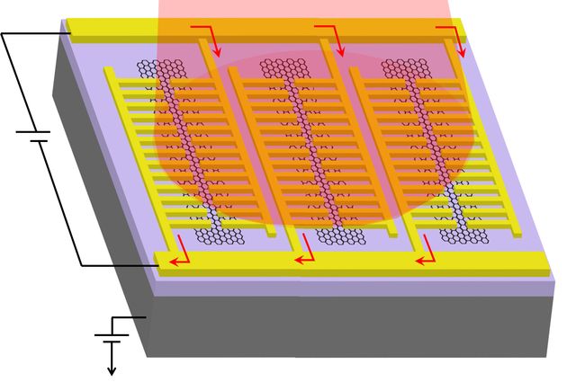
The photodetector operates across a broad range of light, processes images more quickly and is more sensitive to low levels of light than current technology. Image: Jarrahi Research Group/UCLA
The new photodetector takes advantage of the unique properties of graphene, a super-thin material made up of a single layer of carbon atoms. Graphene is an excellent material for detecting photons because it can absorb energy from a broad swath of the electromagnetic spectrum — from ultraviolet light to visible light to the infrared and microwave bands. Graphene is also a very good conductor of electrical current — electrons can flow through it unimpeded.
To form the photodetector, the researchers laid strips of graphene over a silicon dioxide layer, which itself covers a base of silicon. Then, they created a series of comb-like nanoscale patterns, made of gold, with “teeth” about 100 nanometers wide. (A nanometer is one-billionth of a meter.)
The graphene acts as a net to catch incoming photons and then convert them into an electrical signal. The gold comb-shaped nanopatterns quickly transfer that information into a processor, which in turn produces a corresponding high-quality image, even under low-light conditions.
“We specifically designed the dimensions of the graphene nanostripes and their metal patches such that incoming visible and infrared light is tightly confined inside them,” says Semih Cakmakyapan, a UCLA postdoctoral scholar and the lead author of the study. “This design efficiently produces an electrical signal that follows ultrafast and subtle variations in the light’s intensity over the entire spectral range, from visible to infrared.”
The study’s other authors were UCLA graduate students Ping Keng Lu and Aryan Navabi.
The research was supported by the Department of Energy.
Source: UCLA