This is a conventional STM image of a quantum dot, top, compared with an image produced using the new excited-state SMA-STM technique. CREDIT
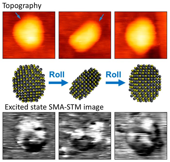
Researchers have developed an imaging technique that uses a tiny, super sharp needle to nudge a single nanoparticle into different orientations and capture 2-D images to help reconstruct a 3-D picture. The method demonstrates imaging of individual nanoparticles at different orientations while in a laser-induced excited state.
The findings, published in The Journal of Chemical Physics, brought together researchers from the University of Illinois and the University of Washington, Seattle in a collaborative project through the Beckman Institute for Advanced Science and Technology at the U. of I.
Nanostructures like microchip semiconductors, carbon nanotubes and large protein molecules contain defects that form during synthesis that cause them to differ in composition from one another. However, these defects are not always a bad thing, said Martin Gruebele, the lead author and an Illinois chemistry professor and chair.
“The term ‘defect’ is a bit of a misnomer,” Gruebele said. “For example, semiconductors are manufactured with intentional defects that form the ‘holes’ that electrons jump into to produce electrical conductivity. Having the ability to image those defects could let us better characterize them and control their production.”
As advances in technology allow for smaller and smaller nanoparticles, it is critical for engineers to know the precise number and location of these defects to assure quality and functionality.
The study focused on a class of nanoparticles called quantum dots. These dots are tiny, near-spherical semiconductors used in technology like solar panels, live cell imaging and molecular electronics – the basis for quantum computing.
The team observed the quantum dots using a single-molecule absorption scanning tunneling microscope fitted with a needle sharpened to a thickness of only one atom at its tip. The needle nudges the individual particles around on a surface and scans them to get a view of the quantum dot from different orientations to produce a 3-D image.
The researchers said there are two distinct advantages of the new SMA-STM method when compared with the current technology – the Nobel Prize-winning technique called cryogenic electron tomography.
For a video related to this research can be found here.
“Instead of an image produced using an average of thousands of different particles, as is done with CryoET, SMA-STM can produce an image from a single particle in about 20 different orientations,” Gruebele said. “And because we are not required to chill the particles to near-absolute zero temperatures, we can capture the particles at room temperature, not frozen and motionless.”
The researchers looked at semiconductor quantum dots for this study, but SMA-STM can also be used to explore other nanostructures such as carbon nanotubes, metal nanoparticles or synthetic macromolecules. The group believes the technique can be refined for use with soft materials like protein molecules, Gruebele said.
The researchers are working to advance SMA-STM into a single-particle tomography technique, meaning that they will need to prove that method is noninvasive.
“For SMA-STM to become a true single-particle tomography technique, we will need to prove that our nudges do not damage or score the nanoparticle in any way while rolled around,” Gruebele said. “Knocking off just one atom can fundamentally alter the defect structure of the nanoparticle.”


