Research & Development World

  • R&D World Home
  • Topics
    • Aerospace
    • Automotive
    • Biotech
    • Careers
    • Chemistry
    • Environment
    • Energy
    • Life Science
    • Material Science
    • R&D Management
    • Physics
  • Technology
    • 3D Printing
    • A.I./Robotics
    • Software
    • Battery Technology
    • Controlled Environments
      • Cleanrooms
      • Graphene
      • Lasers
      • Regulations/Standards
      • Sensors
    • Imaging
    • Nanotechnology
    • Scientific Computing
      • Big Data
      • HPC/Supercomputing
      • Informatics
      • Security
    • Semiconductors
  • R&D Market Pulse
  • R&D 100
    • Call for Nominations: The 2025 R&D 100 Awards
    • R&D 100 Awards Event
    • R&D 100 Submissions
    • Winner Archive
    • Explore the 2024 R&D 100 award winners and finalists
  • Resources
    • Research Reports
    • Digital Issues
    • R&D Index
    • Subscribe
    • Video
    • Webinars
  • Global Funding Forecast
  • Top Labs
  • Advertise
  • SUBSCRIBE

Nanostructuring procedure creates better organic solar cells

By R&D Editors | June 7, 2012

OrganicSolar1

DLIP system (animation) at Fraunhofer IWS. Image: Fraunhofer IWS Dresden

In
recent years the photoelectric efficiency of organic photovoltaics has
made enormous progress. The technology offers the scaling potential to
large and flexible photovoltaic substrates. Further efficiency
improvements are expected from optimizing the intrinsic properties of
the organic material. Micro- and nanostructured surfaces are very
advantageous for organic solar cells since they increase the optical
path length for the incoming light within the active material.

The
scientists at the Fraunhofer IWS apply a very fast and efficient
technology with short processing times at increased resolutions, the
so-called direct laser beam interference pattering method (DLIP). The
method transfers nanostructures in one step into metals, ceramics or
polymers. Making an interference structure requires at least two
collimated and coherent laser beams, which superimpose on the substrate
surface. Interference occurs throughout the entire superposition volume
of the beams. A single laser pulse can process a surface area of up to
several square centimeters, which leads to an effective structuring
speed of several square centimeters per second.

In
close cooperation with the Institute for Applied Photo Physics (IAAP)
of the Technische Universität Dresden the IWS scientists investigated
the influence of the DLIP structuring procedure on the efficiency
improvement of organic cells on PET foils. It proved that the efficiency
of solar cells on structured substrates could be decisively improved.
The superposition of two laser beams results in a linear structure. This
procedure achieves an efficiency increase of approximately 10% compared
to the non-structured PET substrate. Three beams that are not within
the same spatial plane form a point structure. The structuring period is
defined by the angle between two laser beams and their wavelengths.
Crossed structures are made in a two-step process. First a linear
structure is imprinted and then the substrate is rotated by 90 degrees prior to
repeating the same structuring step. This technology turns out to be
especially advantageous for organic cells on PET foils and leads to an
efficiency increase of 21%.

OrganicSolar2

DLIP structured polymer foil. Image: Fraunhofer IWS Dresden
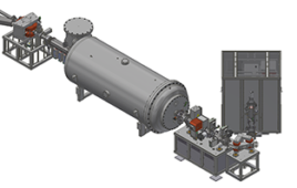
For
the industrial implementation of this procedure the IWS engineers
developed a compact laser interference system, which enables an inline
structuring process. The system and its process principle will be presented at this year’s Lasys in Stuttgart at booth 4.C31.


Source: Fraunhofer Institute of Technology

Related Articles Read More >

Sandia
Sandia Truman Fellows advance quantum optics from lab to wafer-scale and field applications
Sandia National Laboratories’ Kenneth Armijo, project lead, stands beside the Sandia Molten Salt Test Loop, the world’s largest lab-scale molten salt testing facility. (Photo by David Lienemann)
Sandia to restart molten-salt test loop with $2.5 million DOE funding
2025 R&D layoffs tracker tops 92,000
Efficiency first: Sandia’s new director balances AI drive with deterrent work
rd newsletter
EXPAND YOUR KNOWLEDGE AND STAY CONNECTED
Get the latest info on technologies, trends, and strategies in Research & Development.
RD 25 Power Index

R&D World Digital Issues

Fall 2024 issue

Browse the most current issue of R&D World and back issues in an easy to use high quality format. Clip, share and download with the leading R&D magazine today.

Research & Development World
  • Subscribe to R&D World Magazine
  • Enews Sign Up
  • Contact Us
  • About Us
  • Drug Discovery & Development
  • Pharmaceutical Processing
  • Global Funding Forecast

Copyright © 2025 WTWH Media LLC. All Rights Reserved. The material on this site may not be reproduced, distributed, transmitted, cached or otherwise used, except with the prior written permission of WTWH Media
Privacy Policy | Advertising | About Us

Search R&D World

  • R&D World Home
  • Topics
    • Aerospace
    • Automotive
    • Biotech
    • Careers
    • Chemistry
    • Environment
    • Energy
    • Life Science
    • Material Science
    • R&D Management
    • Physics
  • Technology
    • 3D Printing
    • A.I./Robotics
    • Software
    • Battery Technology
    • Controlled Environments
      • Cleanrooms
      • Graphene
      • Lasers
      • Regulations/Standards
      • Sensors
    • Imaging
    • Nanotechnology
    • Scientific Computing
      • Big Data
      • HPC/Supercomputing
      • Informatics
      • Security
    • Semiconductors
  • R&D Market Pulse
  • R&D 100
    • Call for Nominations: The 2025 R&D 100 Awards
    • R&D 100 Awards Event
    • R&D 100 Submissions
    • Winner Archive
    • Explore the 2024 R&D 100 award winners and finalists
  • Resources
    • Research Reports
    • Digital Issues
    • R&D Index
    • Subscribe
    • Video
    • Webinars
  • Global Funding Forecast
  • Top Labs
  • Advertise
  • SUBSCRIBE