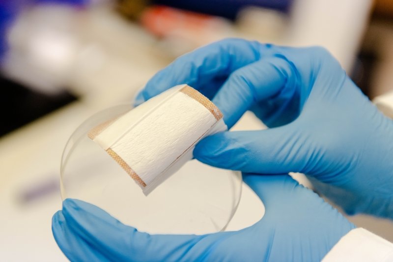
Rao’s team sought to streamline the nanofiber production process.
Biomedical engineers cut post-processing steps to make electrospun nanofibers for wound healing and improve 3D-matrices for biological tissues. They speed up prototyping using identical materials.
Electrospinning uses electric fields to manipulate nanoscale and microscale fibers. The technique is well-developed but time-intensive and costly. A team from Michigan Technological University came up with a new way to create customizable nanofibers for growing cell cultures that cuts out time spent removing toxic solvents and chemicals. Their work is published in Elsevier’s Materialia.
Smitha Rao, assistant professor of biomedical engineering at Michigan Tech, led the research. She said the approach is innovative, “we’re coming at this completely sideways,” and the team focused on streamlining electrospun nanofiber production. Nanofibers are used as scaffolds, made up of strands and pockets, that can grow cells.
“We want an assembled, highly aligned scaffold that has ideal structures and patterns on it that cells will like,” Rao said. “Take a cell, put it on porous materials versus elastic materials versus hard materials, and it turns out the cell does different things. Usually you use varied materials to get these diverse characteristics. Cells respond differently when you put them on different surfaces, so can we make scaffolds that provide these different conditions while keeping the materials the same?”
In a nutshell, yes. And making customizable scaffolds is surprisingly simple, especially when compared to the laborious casting and additive processes typically used to produce scaffolds suitable for electrospinning. Plus, Rao’s team discovered a pleasant side effect.
“We take the polymers, then we put them into solutions, and we came up with this magical formula that works—and then we had to go electrospin it,” Rao explained, adding that the team noticed something odd during the process.
“We saw that the cells aligned without us applying anything externally. Typically, to make them align you have to put them in an electric field, or put them in a chamber and agitate the scaffold to force them to align in a particular direction by applying external stresses,” she said. “We’re basically taking pieces of this scaffold, throwing it in a culture plate and dropping cells on it.”
When spun in an electric field—imagine a cotton candy machine—the self-aligning cells follow the strand-and-pocket pattern of the underlying nanofibers. Rao’s team, including lead author and PhD student Samerender Nagam Hanumantharao and master’s student Carolynn Que, found that varying electric field strengths result in different pocket sizes. At 18 kilovolts, the magic happens and the fibers align just so. At 19 kilovolts, small pockets form, ideal for cardiac myoblasts. At 20 kilovolts, honeycombs of pockets expand in the fibers. Bone cells prefer the pockets formed at 21 kilovolts; dermal cells aren’t picky, but especially like the spacious rooms that grow at 22 kilovolts.
Rao’s team tested a variety of polymer mixes and found that some of the most common materials remain tried-and-true. Their magical two-polymer blend let them manipulate the nanofiber pocket size; a three-polymer blend made tweaking the mechanical properties possible. The polymers include polycaprolactone (PCL), biodegradable and easy to shape, and conductive polyaniline (PANI), which together made a two-polymer blend, which could be combined with polyvinylidene difluoride (PVDF).
“Because polyaniline is conducting in nature, people can throw it into the fiber matrix to get conductive scaffolds for cells such as neurons,” Rao said. “However, no one has used these materials to manipulate the process conditions.”
Being able to use the same materials to create different nanofiber characteristics means eliminating chemical and physical variables that can mess with experimental results. Rao hopes that as more researchers use her team’s blends and process, it will speed up research to better understand neural mechanisms, speed up wound healing technology, test cell lines and boost rapid prototyping in biomedical engineering.
“We’re trying to simplify the process to answer a highly complex question: how do cells proliferate and grow?” Rao said. “This is our basic building block; this is the two-by-two Lego. And you can build whatever you want from there.”