Research & Development World

  • R&D World Home
  • Topics
    • Aerospace
    • Automotive
    • Biotech
    • Careers
    • Chemistry
    • Environment
    • Energy
    • Life Science
    • Material Science
    • R&D Management
    • Physics
  • Technology
    • 3D Printing
    • A.I./Robotics
    • Software
    • Battery Technology
    • Controlled Environments
      • Cleanrooms
      • Graphene
      • Lasers
      • Regulations/Standards
      • Sensors
    • Imaging
    • Nanotechnology
    • Scientific Computing
      • Big Data
      • HPC/Supercomputing
      • Informatics
      • Security
    • Semiconductors
  • R&D Market Pulse
  • R&D 100
    • 2025 R&D 100 Award Winners
    • 2025 Professional Award Winners
    • 2025 Special Recognition Winners
    • R&D 100 Awards Event
    • R&D 100 Submissions
    • Winner Archive
  • Resources
    • Research Reports
    • Digital Issues
    • Educational Assets
    • R&D Index
    • Subscribe
    • Video
    • Webinars
    • Content submission guidelines for R&D World
  • Global Funding Forecast
  • Top Labs
  • Advertise
  • SUBSCRIBE

Scientists Observe Nanowires as They Grow

By Karlsruher Institut Für Technologie (Kit) | March 14, 2018

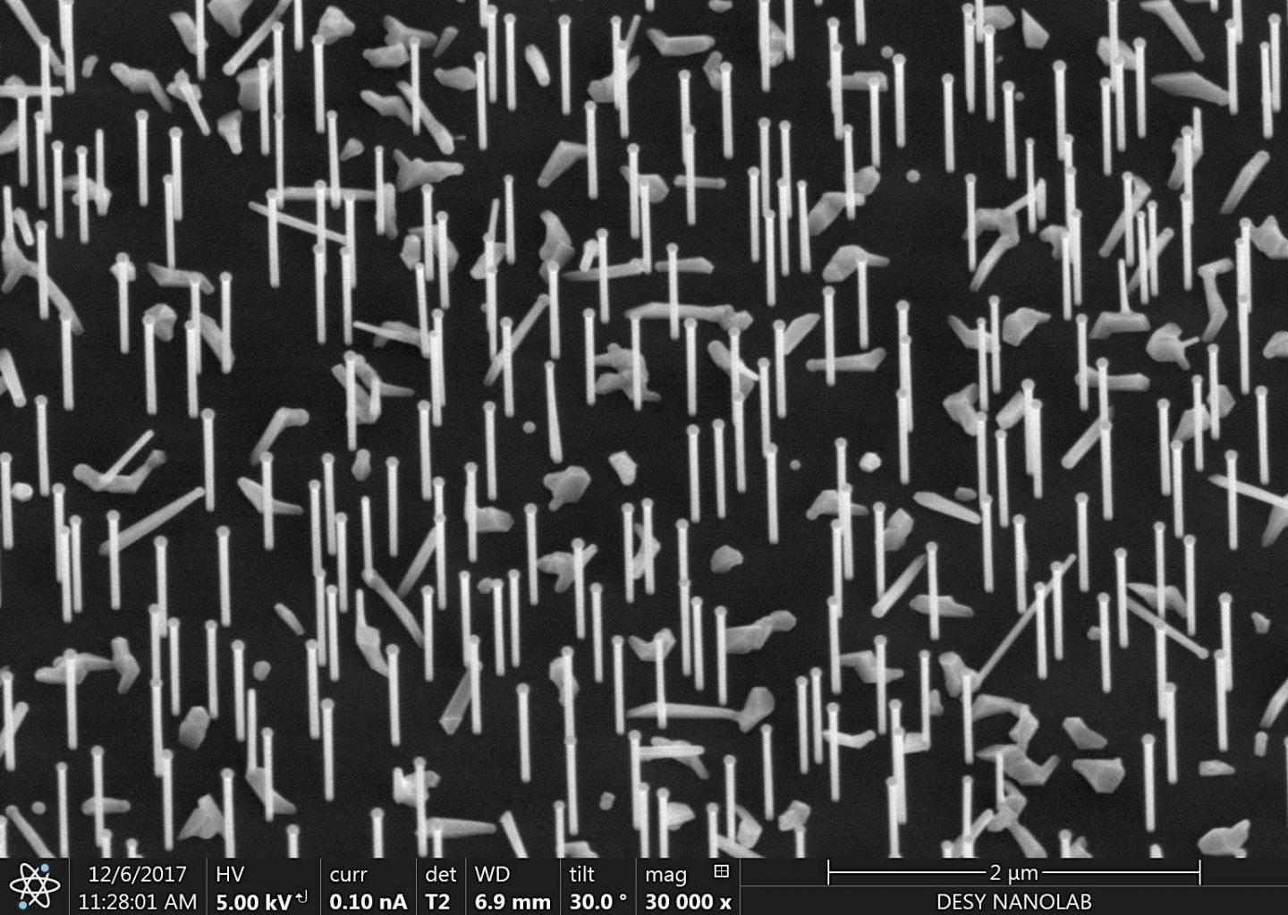
Nanoforest: Nanowires on a silicon wafer as recorded at the DESY NanoLab.

Scientists of Karlsruhe Institute of Technology (KIT) have succeeded in monitoring the growth of minute gallium arsenide wires. Their findings do not only provide for a better understanding of growth, they also enable approaches to customizing nanowires with special properties for certain applications in the future. Gallium arsenide is a semiconductor material widely used in infrared remote controls, high-frequency technology for mobile phones, conversion of electric signals into light in glass-fiber cables, and solar cells for space technology. The results were presented in the journal Nano Letters by the team of Philipp Schroth of KIT and the University of Siegen.

For wire production, the scientists used the self-catalyzed vapor-liquid-solid process (VLS process). Minute liquid gallium droplets are deposited on a hot silicon crystal of around 600°C in temperature. Then, this wafer is subjected to directed beams of gallium atoms and arsenic molecules that dissolve in the gallium droplets. After some time, nanowires start to grow below the droplets that act as catalysts for the longitudinal growth of the wires. “This process is quite well established, but it has been impossible so far to specifically control it. To achieve this, the details of growth have to be understood first,” co-author Ludwig Feigl of KIT says.

For the studies, the team used a portable chamber specifically designed by KIT’s Institute for Photon Science and Synchrotron Radiation (IPS) with funds of the Federal Ministry of Education and Research (BMBF). The researchers installed the chamber in the research light source PETRA III of the German Electron Synchrotron (DESY) and took X-ray pictures every minute to determine the structure and diameter of the growing nanowires. Finally, they measured the fully grown nanowires with an electron microscope. “We found that growth of nanowires is not only caused by the VLS process, but also by a second component that was observed and quantified directly for the first time in this experiment. This so-called side-wall growth makes the wires gain width,” says Philipp Schroth. In the course of the growth process, the gallium droplets become larger due to constant gallium vapor deposition. This has a far-reaching impact. “As the droplet size changes, the contact angle between the droplet and the surface of the wires changes as well. In certain cases, this causes the wire to suddenly continue growing with another crystal structure,” Feigl says. This change is of relevance to applications, as the structure and shape of the nanowires considerably affect the properties of the resulting material.

Publication in Nano Letters: https://pubs.acs.org/doi/10.1021/acs.nanolett.7b03486

Related Articles Read More >

R&D 100 winner LLNL achieves 1,000x speed boost in 3D nanofabrication
CEA-Leti achieves 400°C CMOS fabrication milestone for 3D chip stacking
The 2025 R&D 100 Finalists are here
New nanotechnology method increases microalgae biofuel yield by 300%
rd newsletter
EXPAND YOUR KNOWLEDGE AND STAY CONNECTED
Get the latest info on technologies, trends, and strategies in Research & Development.
RD 25 Power Index

R&D World Digital Issues

Fall 2025 issue

Browse the most current issue of R&D World and back issues in an easy to use high quality format. Clip, share and download with the leading R&D magazine today.

R&D 100 Awards
Research & Development World
  • Subscribe to R&D World Magazine
  • Sign up for R&D World’s newsletter
  • Contact Us
  • About Us
  • Drug Discovery & Development
  • Pharmaceutical Processing
  • Global Funding Forecast

Copyright © 2026 WTWH Media LLC. All Rights Reserved. The material on this site may not be reproduced, distributed, transmitted, cached or otherwise used, except with the prior written permission of WTWH Media
Privacy Policy | Advertising | About Us

Search R&D World

  • R&D World Home
  • Topics
    • Aerospace
    • Automotive
    • Biotech
    • Careers
    • Chemistry
    • Environment
    • Energy
    • Life Science
    • Material Science
    • R&D Management
    • Physics
  • Technology
    • 3D Printing
    • A.I./Robotics
    • Software
    • Battery Technology
    • Controlled Environments
      • Cleanrooms
      • Graphene
      • Lasers
      • Regulations/Standards
      • Sensors
    • Imaging
    • Nanotechnology
    • Scientific Computing
      • Big Data
      • HPC/Supercomputing
      • Informatics
      • Security
    • Semiconductors
  • R&D Market Pulse
  • R&D 100
    • 2025 R&D 100 Award Winners
    • 2025 Professional Award Winners
    • 2025 Special Recognition Winners
    • R&D 100 Awards Event
    • R&D 100 Submissions
    • Winner Archive
  • Resources
    • Research Reports
    • Digital Issues
    • Educational Assets
    • R&D Index
    • Subscribe
    • Video
    • Webinars
    • Content submission guidelines for R&D World
  • Global Funding Forecast
  • Top Labs
  • Advertise
  • SUBSCRIBE