A team of multi-disciplinary scientists and engineers at the University of Illinois at Urbana-Champaign have discovered a new, more precise method to create nanoscale-size electromechanical devices. Their research findings are published in Nature Communications.
“In the last five years, there has been a huge gold rush where researchers figured out we could make 2D materials that are naturally only one molecule thick but can have many different electronic properties, and by stacking them on top of each other, we could engineer nearly any electronic device at molecular sizes,” says Arend van der Zande, professor of mechanical science and engineering.
“The challenge was, though we could make these structures down to a few molecules thick, we couldn’t pattern them,” he says.
At any scale of electronic device, layers are etched away in precise patterns to control how the current flows.
“This concept underlies many technologies, like integrated circuits. However, the smaller you go, the harder this is to do,” says van der Zande.
“For example, how do you make electrical contact on molecular layer three and five, but not on layer four at the atomic level?”
A serendipitous discovery led to a method for doing just that.
As a new postdoctoral researcher in van der Zande’s lab, Jangyup Son was running some experiments on single layers of graphene using Xenon difluoride, XeF2, when he happened to “throw in” another material on hand: hexagonal Boron Nitride (hBN), an electrical insulator.
“Jangyup shoved both materials into the etching chamber at the same time, and what he saw was that a single layer of graphene was still there, but a thick piece of hBN was completely etched away by the Xenon difluoride.”
This accidental discovery led the team to see where they could apply graphene’s ability to withstand the etching agent.
“This discovery allowed us to pattern two-dimensional structures by placing layers of graphene between other materials, such as hexagonal boron nitride (hBN), transition metal dichalcogenides (TMDCs), and black phosphorus (BP), to selectively and precisely etch one layer without etching the layer underneath.”
Graphene, when exposed to the etching agent XeF2, retains its molecular structure and masks, or protects, the layer below and actually stops the etch.
“What we’ve discovered is a way to pattern complicated structures down to a molecular and atomic scale,” he says.

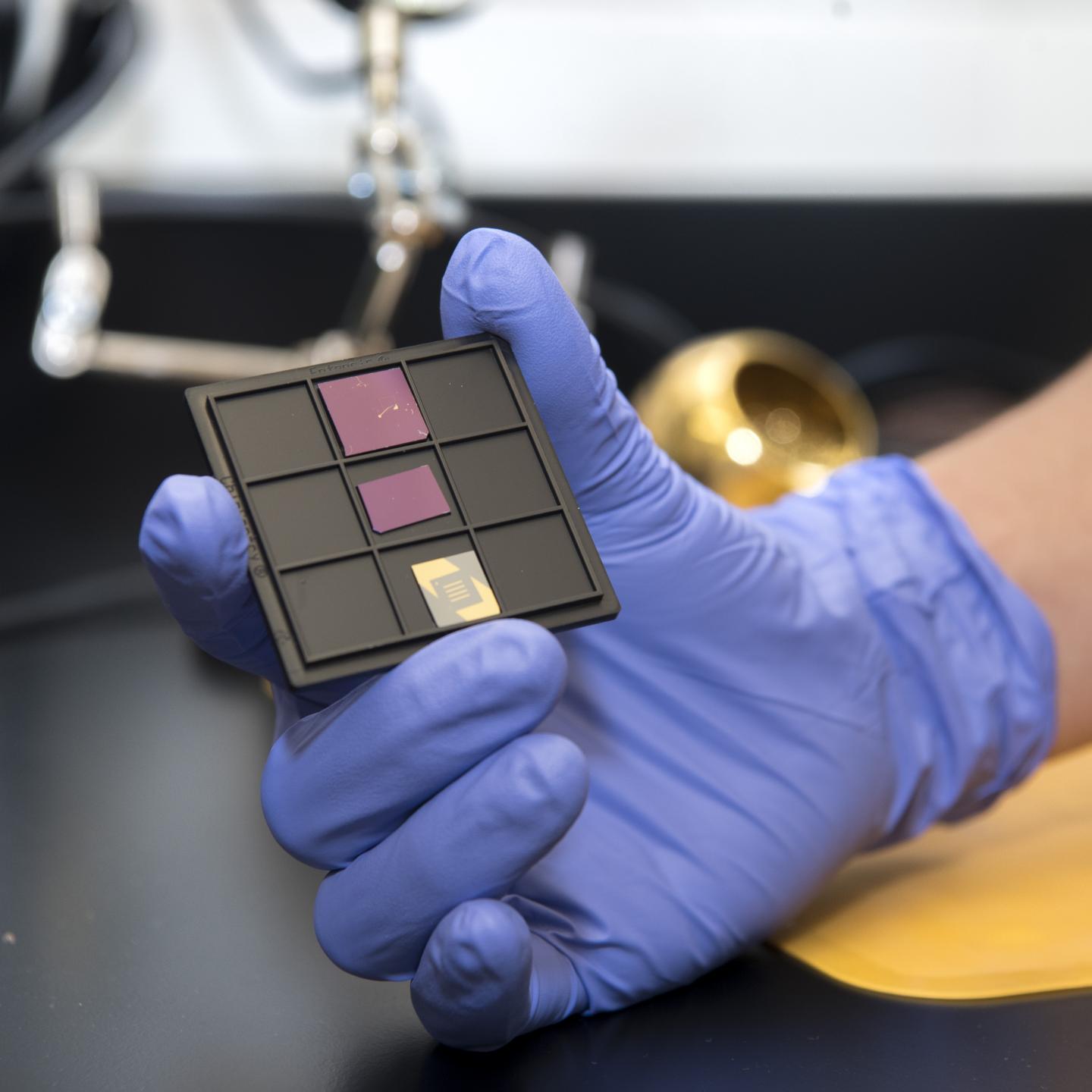
Nanoelectronic devices made from atomically thin materials on a silicon chip. Image: University of Illinois Department of Materials Science and Engineering
To explore the strengths of the new technique, the group created a simple graphene transistor to test its performance relative to traditionally made graphene transistors, which are currently patterned in a way that induces disorder in the material, degrading their performance.
“Because these molecules are all surface, if you have it sitting on anything with any disorder at all, it messes up the ability for the electrons to move through the material and thus the electronic performance,” says van der Zande.
“In order to make the best device possible, you need to encapsulate the graphene molecule in another two-dimensional material such as insulating hBN to keep it super flat and clean.”
This is where the new technique is so useful. The graphene molecule can remain encapsulated and pristine, while withstanding the etching needed to make contact with the material, thereby preserving the material’s properties.
As proof of concept, the transistors made using the new technique out-performed all other transistors, “making them the best graphene transistors so far demonstrated in the literature,” he says.
The next steps, says van der Zande, are to see how scalable the technique is and whether it will enable previously impossible devices. Can we take advantage of the self-arresting nature of this technique to make a million identical transistors rather than just one? Can we pattern devices down to the nanoscale in all three dimensions at the same time to make nanoribbons without any disorder?
“Now that we have a way of minimizing the disorder within the material, we are exploring ways to make smaller features because we can do encapsulation and patterning at the same time,” he says. “Normally, when you try to make smaller features like nanoribbons of 2D materials the disorder begins to dominate, so the devices do not work properly.”
“The graphene etch stop, as the technique is called, will make the entire process of building devices easier.”
The research involved a multi-disciplinary collaboration of people and shared facilities equipment from the Materials Research Laboratory and the Micro & Nanotechnology Lab. Expert faculty include: Associate Professor of Physics and Director of the Illinois Materials Research Science and Engineering Center (MRSEC), Nadya Mason, for electronic transport; Associate Professor of Mechanical Science and Engineering, Elif Ertekin, for modeling interfaces; and Assistant Professor of Materials Science and Engineering, Pinshane Huang, for electron microscopy. MRSEC provided the primary funding for this research.


