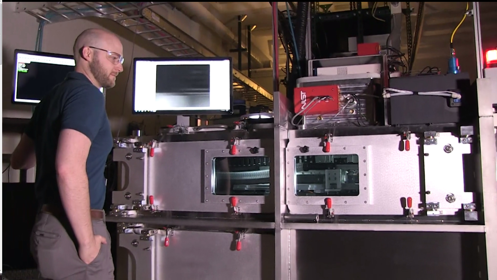
This is a screenshot from a video about NIST’s 3D printer testbed. This 3D printer builds objects by melting a fine metal powder with a laser. First, the surface is coated with metal powder. Then, a high-power laser melts that powder in a particular pattern. The process is repeated hundreds or thousands of times, building the metal piece layer by layer. Finally, when the object is complete, the excess powder is removed. NIST researchers are studying this kind of 3D printing to give industry users tools for more control over their own 3D printing processes.
3D printing of metal objects is a booming industry, with the market for products and services worth more than an estimated $2.3 billion in 2015 – a nearly five-fold growth since 2010. For this type of manufacturing, a metal part is built up successively, layer by layer, over minutes or hours. Sometimes thousands of layers are added together to make a single piece – a reason why this process is conventionally referred to as “additive manufacturing” (AM).
Additive manufacturing machines are particularly handy for making objects with complex forms or geometry, or internal features like ducts or channels. They are becoming increasingly popular in the aerospace, automotive, medical, and technology industries, to make complex pieces such as fuel injector nozzles for engines or titanium bone implants for skull, hip, and other repairs.
But the commercial technology is still relatively new, and maintaining quality control can be challenging and time-consuming. Two products made in the same way on the same machine don’t necessarily come out with the same dimensions, says NIST’s Brandon Lane. Tiny imperfections referred to as pores can appear in the layers, reducing the strength properties of the part. Residual stresses can build up as the layers cool, creating cracks between layers and warping the piece. The stress can be so high, in fact, that it can warp a 1-inch thick piece of steel by a millimeter.
“It will actually break bolts inside the machine, because it just wants to potato chip up from the residual stress,” Lane says. “Anyone who has a commercial machine has seen parts just rip up off of the plate.”
What AM users need is more control over the 3D printing process, and that means answering some fundamental questions. How hot does the melting metal get in each layer? How do you lower the stresses that cause cracking and warping? And what sensors would you need in order to provide better information about what’s happening inside the printing machine?
To address these issues, researchers from two NIST laboratories – NIST’s Engineering Laboratory (EL) and Physical Measurement Laboratory (PML) – have teamed up to build the Additive Manufacturing Metrology Testbed (AMMT), a custom-made 3D printer that they can use to better understand AM processes. Their goal is to study the process in depth and produce the tools that users need to monitor the process in real time.
“In the additive manufacturing realm, there was already a push in industry to start incorporating sensors and monitoring systems on their machines,” says Lane, a member of the Engineering Laboratory (EL). “So we wanted to be able to have that capability, and we also wanted a platform where we could test completely new ideas” for sensors.
The 3D printer testbed system they designed is about the size of a small car and works in the same way as many commercial AM systems of this type. A mechanical arm applies a thin, even layer of metal powder to the surface of a flat metal plate. Then a high-power laser beam moves across the surface of this dusting of metal in the pattern needed for the piece being manufactured. The laser melts the powder, which briefly liquefies before cooling into a solid. When the laser is finished, a new layer of powder is applied, and the process repeats.
At the end, any excess powder – which could be under or inside areas of the piece – is removed, leaving the finished metal object standing alone. Currently, the machine is set up to use three different metals common to commercial AM machines: stainless steel, cobalt chrome, and a nickel alloy. (See video for demonstration.)
Unlike commercial systems, whose software is proprietary, the NIST testbed gives researchers complete control over the system. “Commercial systems are a little bit ‘black box,’” Lane says. “You can command a certain laser power and velocity, but you really don’t have control over every single microsecond of the process. With our system, we can control the speed and power of the laser at 100 kilohertz – that’s every 10 microseconds.” Lane and his EL and PML colleagues designed and built the testbed itself. EL will be largely responsible for running the tests on the system, while PML researchers have been working to supply the sensors for the measurements of the process as well as calibrations and traceability to national standards.
Since many of the AM process problems occur during melting, the NIST team needed to find a way to precisely monitor the temperature of what they call the “melt pool” – the pool of molten metal liquid produced while the laser is heating up the powder. In this case, the best way to gauge its temperature is to measure properties of the light coming off of it. Materials heat up to different colors depending on how hot they are – which is why lava is a deep red and our sun is yellow-white.
For now, they are set up to measure brightness – which they say may be enough for many AM users. “They may only want relative measurements – relative observations of the melt pool fluctuations,” Lane says. But the ultimate goal is to turn those relative measurements into absolute measurements – to use brightness and other properties as a way to gauge the actual temperature of the melt pool. To do this, PML staff will need to characterize the system and ensure that the light intensity sensors have been well-calibrated with standards.
“Eventually we’ll want to get to a full temperature map of the surface” over a wide range of light wavelengths, Lane says, from blue visible light at about 400 nm to mid-infrared (IR) light at 10 microns, which has wavelengths that are too long for the human eye to see. “PML is essential for helping us to do that.”
Currently, the researchers are using a camera with a custom-designed achromatic lens to measure the pool’s brightness over some of the wavelengths they will eventually need, from reddish to near-IR light, at about 850 nm. “But at the higher and higher temperatures, it’s the bluer light – the shorter-wavelength visible light – that matters,” PML’s Steve Grantham says. “So we’ll actually have some different diagnostics” to measure that.
The addendum sensor system he and his PML colleagues will create over the next year and a half is called the Temperature and Emittance of Melts, Powders, and Solids (TEMPS). Among its many capabilities, the system will include a reflectometer in the shape of a hemisphere, which will allow them to collect information about the light reflecting off of the melt pool. The reflectometer will in turn enable them to map the emittance of the melt pool as well as its changing temperatures over time. And TEMPS will include spectrographs, permitting measurement of the full visible and IR spectrum out to wavelengths of 10 microns.
“When the TEMPS system comes in, we’re going to get three times the magnification and expanded wavelength regime,” Lane says.
In the coming years, there is plenty of room to expand their capabilities further, the researchers say. “Right now, [we’re] looking at three basic materials, but anything that anybody’s using in additive manufacturing is fair game,” Grantham says. And eventually, they hope the system will be useful beyond additive manufacturing, to look at solid materials that experience extreme heat, such as the wingtips of supersonic aircraft.


