Research & Development World

  • Home Page
  • Topics
    • Aerospace
    • Archeology
    • Automotive
    • Biotech
    • Chemistry
    • COVID-19
    • Environment
    • Energy
    • Life Science
    • Material Science
    • R&D Market Pulse
    • R&D Management
    • Physics
  • Technology
    • 3D Printing
    • A.I./Robotics
    • Battery Technology
    • Controlled Environments
      • Cleanrooms
      • Graphene
      • Lasers
      • Regulations/Standards
      • Sensors
    • Imaging
    • Nanotechnology
    • Scientific Computing
      • Big Data
      • HPC/Supercomputing
      • Informatics
      • Security
      • Software
    • Semiconductors
  • 2021 R&D 100 Award Winners
    • R&D 100 Awards
    • 2020 Winners
    • Winner Archive
  • Resources
    • Digital Issues
    • Podcasts
    • Subscribe
  • Global Funding Forecast
  • Webinars

Air Gaps Key to Next-Gen Nanochips

By Kenny Walter | November 19, 2018

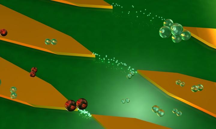
The nano-gap transistors operating in air. As gaps become smaller than the mean-free path of electrons in air, there is ballistic electron transport. Credit: RMIT University

A new type of transistor—which uses air gaps to eliminate the need for semiconductors—could help scientists produce more efficient nanochips.

RMIT University researchers have engineered a new type of transistor that send electrons through narrow air gaps where they can travel unimpeded, rather than sending electrical currents through silicon.

“Every computer and phone has millions to billions of electronic transistors made from silicon, but this technology is reaching its physical limits where the silicon atoms get in the way of the current flow, limiting speed and causing heat,” lead author and PhD candidate in RMIT’s Functional Materials and Microsystems Research Group Shruti Nirantar said in a statement. “Our air channel transistor technology has the current flowing through air, so there are no collisions to slow it down and no resistance in the material to produce heat.”

While the power of computer chips has doubled about every two years for decades, recently the progress has stalled as engineers struggle to make smaller transistor parts.

However, the researchers believe the new device is a promising way to create nano electronics that respond to the limitations of silicon-based electronics. Traditional solid channel transistors are packed with atoms, causing the electrons passing through them to collide and slow down to waste energy as heat.

“Imagine walking on a densely crowded street in an effort to get from point A to B,” research team leader Associate Professor Sharath Sriram, PhD, said in a statement. “The crowd slows your progress and drains your energy.

“Travelling in a vacuum on the other hand is like an empty highway where you can drive faster with higher energy efficiency,” he added.

However, vacuum-packaging solutions around transistors has not been a feasible option because, while it makes them faster, it also increases their size.

“We address this by creating a nanoscale gap between two metal points,” Sriram said. “The gap is only a few tens of nanometers, or 50,000 times smaller than the width of a human hair, but it’s enough to fool electrons into thinking that they are travelling through a vacuum and re-create a virtual outer-space for electrons within the nanoscale air gap.”

The researchers aim to develop the device to be compatible with modern industry fabrication and development processes. Along with electronic applications, the transistors could be used in the aerospace industry to create electronics resistant to radiation and to use electron emission for steering and positioning nano-satellites.

“This is a step towards an exciting technology which aims to create something out of nothing to significantly increase speed of electronics and maintain pace of rapid technological progress,” Sriram said.

The study was published in Nano Letters.  


Related Articles Read More >

Glowing rocks, a new sport, and what we can learn about different approaches
R&D winner of the day: Monolithic Fiber Array Launcher
R&D collaborations looking to build expertise, in this week’s R&D power index
Invention addresses the problems of running a red light at traffic intersections
2021 R&D Global Funding Forecast

Need R&D World news in a minute?

We Deliver!
R&D World Enewsletters get you caught up on all the mission critical news you need in research and development. Sign up today.
Enews Signup

R&D World Digital Issues

February 2020 issue

Browse the most current issue of R&D World and back issues in an easy to use high quality format. Clip, share and download with the leading R& magazine today.

Research & Development World
  • Subscribe to R&D World Magazine
  • Enews Sign Up
  • Contact Us
  • About Us
  • Drug Discovery & Development
  • Pharmaceutical Processing
  • 2022 Global Funding Forecast

Copyright © 2022 WTWH Media LLC. All Rights Reserved. The material on this site may not be reproduced, distributed, transmitted, cached or otherwise used, except with the prior written permission of WTWH Media
Privacy Policy | Advertising | About Us

Search R&D World

  • Home Page
  • Topics
    • Aerospace
    • Archeology
    • Automotive
    • Biotech
    • Chemistry
    • COVID-19
    • Environment
    • Energy
    • Life Science
    • Material Science
    • R&D Market Pulse
    • R&D Management
    • Physics
  • Technology
    • 3D Printing
    • A.I./Robotics
    • Battery Technology
    • Controlled Environments
      • Cleanrooms
      • Graphene
      • Lasers
      • Regulations/Standards
      • Sensors
    • Imaging
    • Nanotechnology
    • Scientific Computing
      • Big Data
      • HPC/Supercomputing
      • Informatics
      • Security
      • Software
    • Semiconductors
  • 2021 R&D 100 Award Winners
    • R&D 100 Awards
    • 2020 Winners
    • Winner Archive
  • Resources
    • Digital Issues
    • Podcasts
    • Subscribe
  • Global Funding Forecast
  • Webinars