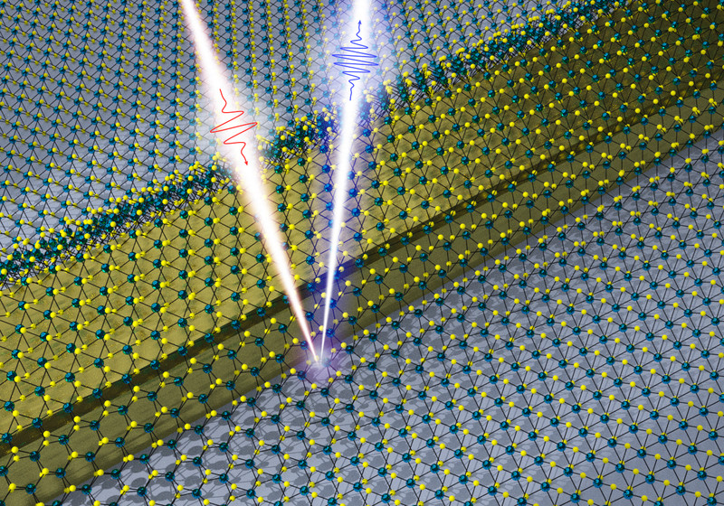
The basic idea of the measurement method: red light hits the surface — blue light is sent back.
Two-dimensional materials such as graphene, which consist of only one or a few atomic layers, have been a very promising aspect of materials science over recent years. They demonstrate remarkable properties that open up completely new technical possibilities, from sensor technology to solar cells.
However, there is one important phenomenon that could not be measured accurately up until now: the extreme internal stresses and strains that such materials may be subjected to, which often drastically alter the material’s physical properties. TU Wien has now successfully measured these distortions in 2D materials at microscopic level, which means it is now possible to observe precisely (point for point) how the properties of a material may be altered as a result of a simple distortion. These new measurement methods have now been published in the specialist journal Nature Communications.
When a material is stretched or compressed, the distance between the individual atoms changes, and this distance has an influence on the electronic properties of the material. This phenomenon has been used in semiconductor technology for years: silicon crystals, for example, can be grown so that they are permanently under internal mechanical stress.
However, two-dimensional materials, which consist only of an ultra-thin layer, offer much greater potential: “A crystal can be stretched by perhaps one percent before it breaks. With 2D materials, deformation of ten or twenty percent is possible,” says Professor Thomas Müller from the Photonics Institute (Faculty of Electrical Engineering and Information Technology) at TU Wien. Depending on the deformation and mechanical stresses present within the material, the electronic properties may completely change, such as the ability of the electrons to absorb incoming light.
“Up until now, if you wanted to measure stresses present in this type of material you had to rely on extremely complicated measurement methods,” explains Lukas Mennel (TU Wien), lead author of the publication. For example, you could observe the surface using a transmission electron microscope, measure the average distance between the atoms and then deduce any stretching or compression from that. At TU Wien, this process has now been made much simpler and more accurate.
Here, a remarkable effect called frequency doubling is used: “If you irradiate specific materials — in our case a layer of molybdenum disulphide — with a suitable laser beam, the material may reflect back light of a different color,” explains Thomas Müller. Two photons in the incoming laser beam are combined to form one photon with double the energy, which is emitted from the material.
However, the intensity of this effect depends on the internal symmetry of the material. Usually, molybdenum disulphide has a honeycomb-like structure, i.e. hexagonal symmetry. If the material is stretched or compressed, this symmetry is slightly distorted — and this small distortion has a dramatic effect on the intensity of the light reflected back from the material.
If you place a layer of molybdenum disulphide over a microstructure, like putting a rubber blanket over a climbing frame, the result is a complex pattern of local distortions. You can now use a laser to scan the material point for point and thus obtain a detailed map of these stretches and compressions. “In doing so, not only can we measure the severity of these deformations, but we can also see the exact direction in which they run,” explains Mennel.
These imaging methods can now be used for the local, targeted adjustment of material properties. “For example, custom material deformations in solar cells could ensure that free charge carriers are diffused away in the right direction as quickly as possible,” says Müller. This research on 2D materials means that a new, powerful tool is now available.
Source: Technische Universität Wien


