Research & Development World

  • R&D World Home
  • Topics
    • Aerospace
    • Automotive
    • Biotech
    • Careers
    • Chemistry
    • Environment
    • Energy
    • Life Science
    • Material Science
    • R&D Management
    • Physics
  • Technology
    • 3D Printing
    • A.I./Robotics
    • Software
    • Battery Technology
    • Controlled Environments
      • Cleanrooms
      • Graphene
      • Lasers
      • Regulations/Standards
      • Sensors
    • Imaging
    • Nanotechnology
    • Scientific Computing
      • Big Data
      • HPC/Supercomputing
      • Informatics
      • Security
    • Semiconductors
  • R&D Market Pulse
  • R&D 100
    • Call for Nominations: The 2025 R&D 100 Awards
    • R&D 100 Awards Event
    • R&D 100 Submissions
    • Winner Archive
    • Explore the 2024 R&D 100 award winners and finalists
  • Resources
    • Research Reports
    • Digital Issues
    • R&D Index
    • Subscribe
    • Video
    • Webinars
  • Global Funding Forecast
  • Top Labs
  • Advertise
  • SUBSCRIBE

Changing and Rearranging Semiconductors Avoids Production Problems

By R&D Editors | October 17, 2017

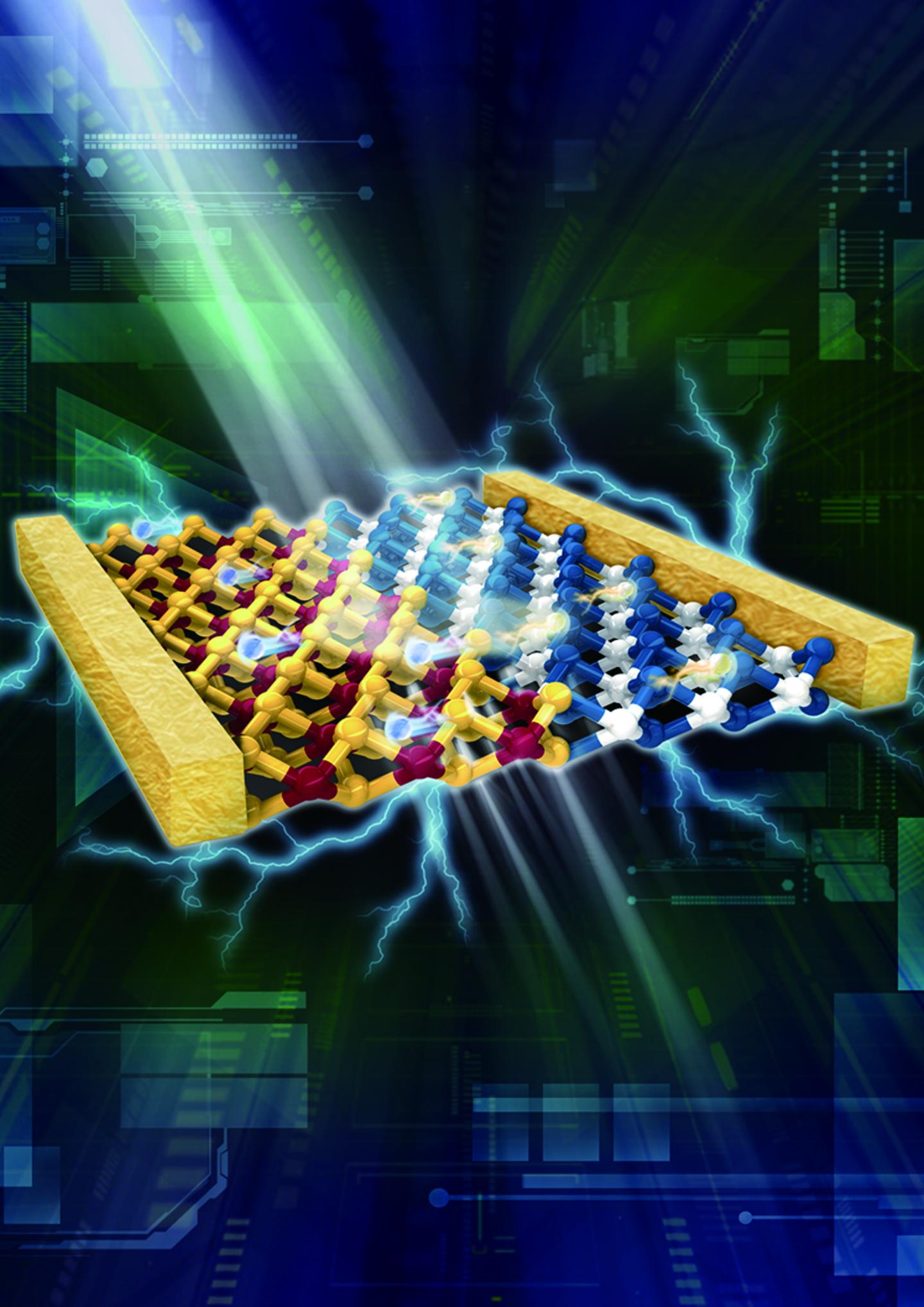
Solar power conversion using a lateral WSe2–MoS2­ heterojunction. Image: © 2017 WILEY VCH

Super thin photovoltaic devices underpin solar technology and gains in the efficiency of their production are therefore keenly sought. King Abdullah University of Science and Technology (KAUST) researchers have combined and rearranged different semiconductors to create so-called lateral p-n heterojunctions — a simpler process they hope will transform the fabrication of solar cells, self-powered nanoelectronics, as well as ultrathin, transparent, flexible devices.

Two-dimensional semiconductor monolayers, such as graphene and transition-metal dichalcogenides like WSe2 and MoS2, have unique electrical and optical properties that make them potential alternatives to conventional silicon-based materials. Recent advances in material growth and transfer techniques have allowed scientists to manipulate these monolayers. Specifically, vertical stacking has led to ultrathin photovoltaic devices but requires multiple complex transfer steps. These steps are hampered by various issues, such as the formation of contaminants and defects at the monolayer interface, which limit device quality.

“Devices obtained using these transfer techniques are usually unstable and vary from sample to sample,” says lead researcher and former visiting student of Associate Professor, Jr-Hau He, Meng-Lin Tsai, who adds that transfer-related contaminants significantly affect device reliability. Electronic properties have also proven difficult to control by vertical stacking.

To fully harness the exceptional properties of these two-dimensional materials, Tsai’s team, under the mentorship of He, created monolayers featuring lateral WSe2-MoS2 heterojunctions and incorporated them into solar cells. Under simulated sunlight, the cells achieved greater power conversion efficiency than their vertically stacked equivalents.

To do this, first the researchers synthesized the heterojunctions by consecutively depositing WSe2 and MoS2 on a sapphire substrate. Next, they transferred the materials onto a silicon-based surface for photovoltaic device fabrication.

High-resolution microscopy revealed that the lateral junction displayed a clear separation between the semiconductors at the interface. Also, the researchers detected no discernable height difference between semiconductor regions, consistent with an atomically thin interface.

These interfacial characteristics signaled success. “Our structures are cleaner and more ideal than vertically stacked assemblies because we didn’t need the multi-step transfer procedure,” explains Tsai.

Furthermore, the lateral heterojunctions mostly retained their efficiency despite changes to the orientation of the incident light. Being able to take light coming from any direction means expensive solar tracking systems will become redundant.

According to Tsai, the implementation of lateral heterojunctions in more complex circuits and interconnects may result in higher performance than in conventional solar cells and so the team is working on the next steps. “We are trying to understand the underlying kinetics and thermodynamics of these heterojunctions to design more efficient cells,” he adds.

Source: King Abdullah University of Science and Technology

Related Articles Read More >

TSMC’s N3P hits mass production, with N3X customer sampling slated for Q3–Q4 2025a
7 major R&D developments this week: Tariff uncertainty persists, Pfizer sells campus, Scania acquires Northvolt unit
While Trump tariffs spare phones/PCs, R&D could faces GPU cost pressures
Why IBM predicts quantum advantage within two years
rd newsletter
EXPAND YOUR KNOWLEDGE AND STAY CONNECTED
Get the latest info on technologies, trends, and strategies in Research & Development.
RD 25 Power Index

R&D World Digital Issues

Fall 2024 issue

Browse the most current issue of R&D World and back issues in an easy to use high quality format. Clip, share and download with the leading R&D magazine today.

Research & Development World
  • Subscribe to R&D World Magazine
  • Enews Sign Up
  • Contact Us
  • About Us
  • Drug Discovery & Development
  • Pharmaceutical Processing
  • Global Funding Forecast

Copyright © 2025 WTWH Media LLC. All Rights Reserved. The material on this site may not be reproduced, distributed, transmitted, cached or otherwise used, except with the prior written permission of WTWH Media
Privacy Policy | Advertising | About Us

Search R&D World

  • R&D World Home
  • Topics
    • Aerospace
    • Automotive
    • Biotech
    • Careers
    • Chemistry
    • Environment
    • Energy
    • Life Science
    • Material Science
    • R&D Management
    • Physics
  • Technology
    • 3D Printing
    • A.I./Robotics
    • Software
    • Battery Technology
    • Controlled Environments
      • Cleanrooms
      • Graphene
      • Lasers
      • Regulations/Standards
      • Sensors
    • Imaging
    • Nanotechnology
    • Scientific Computing
      • Big Data
      • HPC/Supercomputing
      • Informatics
      • Security
    • Semiconductors
  • R&D Market Pulse
  • R&D 100
    • Call for Nominations: The 2025 R&D 100 Awards
    • R&D 100 Awards Event
    • R&D 100 Submissions
    • Winner Archive
    • Explore the 2024 R&D 100 award winners and finalists
  • Resources
    • Research Reports
    • Digital Issues
    • R&D Index
    • Subscribe
    • Video
    • Webinars
  • Global Funding Forecast
  • Top Labs
  • Advertise
  • SUBSCRIBE