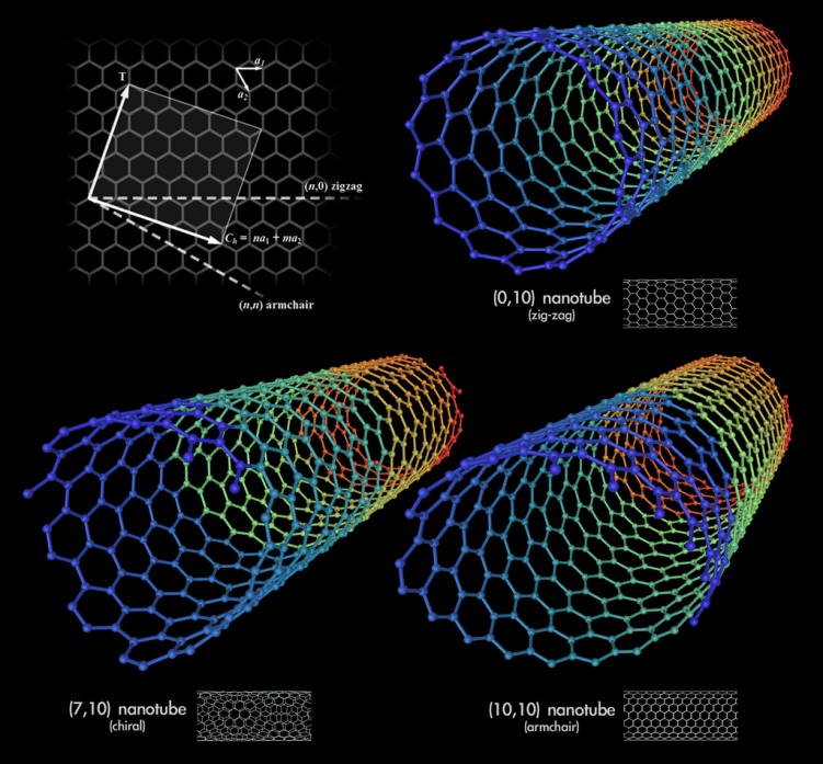
Different types of nanotubes: 1) zigzag, 2) chiral, and 3) armchair (or dentated). Image: NUST MISIS
Scientists from the NUST MISIS Laboratory of Inorganic Nanomaterials, together with their international colleagues, have proved it possible to change the structural and conductive properties of nanotubes by stretching them.
This can potentially expand nanotubes’ application into electronics and high-precision sensors such as microprocessors and high-precision detectors.
The research article has been published in Ultramicroscopy.
Carbon nanotubes can be represented as a sheet of graphene rolled in a special way. There are different ways of “folding” it, which leads to the graphene edges interconnecting at different angles, forming either armchair, zigzag, or chiral nanotubes.
Nanotubes are considered to be promising materials for use in electronics and sensors because they have high electrical conductivity, which would work well in things like microprocessors and high-precision detectors.
However, when producing carbon nanotubes it is hard to control their conductivity. Nanotubes with metallic and semiconducting properties can grow into a single array while microprocessor-based electronics require semiconducting nanotubes that have the same characteristics.
Scientists from the NUST MISIS Laboratory of Inorganic Nanomaterials jointly with a research team from Japan, China and Australia, led by Professor Dmitri Golberg, have proposed a method that allows for the modification of the structure of ready-made nanotubes and thus changes their conductive properties.
“The basis of the nanotube — a folded layer of graphene — is a grid of regular hexagons, the vertices of which are carbon atoms. If one of the carbon bonds in the nanotube is rotated by 90 degrees, a pentagon and a heptagon are formed at this [junction] instead of a hexagon, and a so-called Stone-Wales defect is obtained in this case,” says Associate Professor Pavel Sorokin, Doctor of Physical & Mathematical Sciences and head of the Theoretical Materials Science of Nanostructures infrastructure project at the NUST MISIS Laboratory of Inorganic Nanomaterials.
“Such a defect can occur in the structure under certain conditions. Back in the late 90s, it was predicted that the migration of this defect along the walls of a highly heated nanotube with the application of mechanical stress could lead to a change in its structure — a sequential change in the chirality of the nanotube, which leads to a change in its electronic properties.
“No experimental evidence for this hypothesis has previously been obtained, but our research paper has presented convincing proof of it.”
Scientists from the NUST MISIS Laboratory of Inorganic Nanomaterials have conducted simulations of the experiment at the atomic level.
At first, the nanotubes were lengthened to form the first structural defect consisting of two pentagons and two heptagons (a Stone-Wales defect), where the prolonged lengthening of the tube began to “spread” to the sides, rearranging other carbon bonds.
It was at this stage that the structure of the nanotubes changed. With further stretching, more and more Stone-Wales defects began to form, eventually leading to a change in the nanotubes’ conductivity.
“We were responsible for the theoretical modeling of the process on a supercomputer in the NUST MISIS Laboratory for Modeling and Development of New Materials for the experimental part of the work. We are glad that the simulation results [support] the experimental data,” says Dmitry Kvashnin, co-author of the research work, Candidate of Physical & Mathematical Sciences and a researcher at the NUST MISIS Laboratory of Inorganic Nanomaterials.
The proposed technology is capable of helping in the transformation of “metallic” nanotubes’ structure for their further application in semiconductor electronics and sensors such as microprocessors and ultrasensitive detectors.
Source: NUST MISIS