Artist’s impression of a diamond quantum sensor. The ‘spotlight’ represents light passing through the diamond defect and detecting the movement of electrons. Electrons are shown as red spheres, trailed by red threads that reveal their path through graphene (a single layer of carbon atoms). Picture: David A. Broadway/cqc2t.org
For the first time ever, scientists were able to peek inside of graphene and view electronic currents.
Lloyd Hollenberg, deputy director of the Centre for Quantum Computation and Communication Technology (CQC2T) at the University of Melbourne, led a team to develop a special quantum probe— based on an atomic sized color center found only in diamonds— to enable researchers to see the flow of electric currents in graphene.
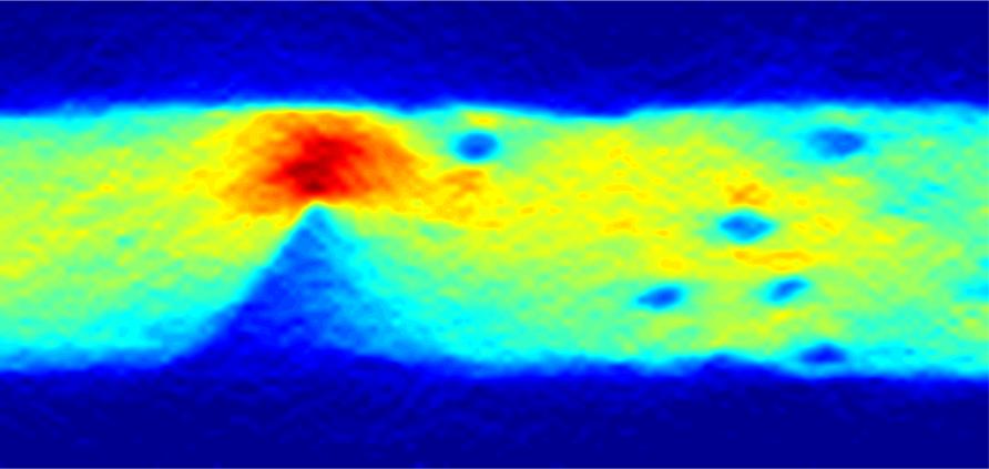
“Our experiment combines, for the first time, quantum sensing and graphene science,” Hollenberg said in an exclusive interview with R&D Magazine. “Namely, we use tiny quantum sensors, in the form of atomic defects in a diamond, to image the flow of electric currents in a graphene device, revealing how the flow is disrupted by minute cracks and defects.
“Our team has been developing quantum sensing techniques and instruments, trying to harness quantum systems and principles in order to make new types of multimodal sensors offering an unprecedented combination of high spatial resolution and sensitivity.”
Lead author Jean-Philippe Tetienne, Ph.D., from CQC2T at the University of Melbourne, explained how they were able image the electrical current in graphene.
“Our method employs a diamond-based quantum sensing platform, which consists of a diamond chip engineered with an array of atomic defects known as nitrogen-vacancy centres,” Tetienne said, in an interview with R&D Magazine. “Each of these defects acts as a tiny magnetic field sensor by precise control and measurement of the energy of its quantum spin state.”
According to Tetienne, the measurement relies on an analysis of the red fluorescence light emitted by the probes, which is subject to a specific combination of green laser light and microwave radiation.
The researchers were able to obtain an image of the electron flow in a conductor based on the phenomenon that an electric current gives rise to a magnetic field.
By measuring and mapping the magnetic field using a quantum sensor array the researchers were able to reconstruct the current density in the conductor.
Tetienne explained some of the challenges they faced.
“The major challengeis that the sample to be measured must be brought close enough to the diamond chip quantum sensor,” he said. “To achieve this, we transferred the graphene layer directly onto the diamond and fabricated the devices using relatively standard microfabrication techniques.”
Hollenberg said the technique to image electric currents is non-invasive and offers high spatial resolution, while working under ambient conditions.
The ability to see how electric currents are affected by imperfections allow researchers to improve the reliability and performance of existing and emerging electronics, including for devices based on atomically-thin materials and structures that are vulnerable to imperfections.
Hollenberg also said the technique could be used to investigate more exotic electric phenomena in graphene or other 2D materials, particularly in the quantum transport regime where electrons obey different laws. Some of the applications include electronics, sensing or quantum computing.
According to the researchers, the ability to conduct electricity enables graphene to be used in solar cells, touch panels and flexible electronics. Graphene can also be used for quantum computers to perform memory and processing tasks and perform certain calculations faster than a conventional computer can.
Tetienne said the next step is to use the technique to investigate the operation of graphene-based transistors, where an electric voltage modulates the current flow, and to study electronic transport in graphene in the quantum regime.
The researchers also plan to apply the technique to better understand conduction in atomically-defined nanostructures in silicon, which could aid future understanding of quantum computers.
“Since the discovery of graphene, which is only one atom thick, there have been tremendous efforts worldwide to develop new tools and instruments allowing researchers to image graphene and characterise its properties, which has been key in advancing the understanding of graphene,” Hollenberg said. “A lot remains to be learnt about graphene, however, especially when it is integrated into complex devices for practical applications, and innovative techniques such as ours will contribute to facilitate new discoveries.”


