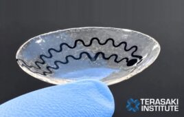
Case Western Reserve University researchers have won a $1.2 million grant to develop technology for mass-producing flexible electronic devices at a whole new level of small.
As they’re devising new tools and techniques to make wires narrower than a particle of smoke, they’re also creating ways to build them in flexible materials and package the electronics in waterproofing layers of durable plastics.
The team of engineers, who specialize in different fields, ultimately aims to build flexible electronics that bend with the realities of life: Health-monitoring sensors that can be worn on or under the skin and foldable electronic devices as thin as a sheet of plastic wrap. And, further down the road, implantable nerve-stimulating electrodes that enable patients to regain control from paralysis or master a prosthetic limb.
Thinking bigger, the team believes the technology could be used to crank out rolls of thin-film solar panels that stand up to decades in the elements. Current thin-film panels are plagued with short life spans due to seepage between layers.
“The commercial development of nanoelectromechanical systems is limited by access to low-cost, high output—we call it ‘throughput’—processing tools,” says Christian Zorman, an associate professor of electrical engineering and computer science and lead researcher on the grant. “We’re trying to address that bottleneck.”
With this four-year National Science Foundation Scalable Nanomanufacturing Program grant, Zorman and his colleagues will push alternative technologies they’ve created to make wires and other metal structures less than 100 nm.
Currently, devices that combine electronic and mechanical functions are being made this small using electron beam lithography. But electron beams are too energetic to use on flexible plastics and require very high vacuum, which significantly limits throughput, is costly, and very time-consuming—all impediments to mass production.
Using inkjet printers to build small devices has proven cheap and effective, but getting down into the nanometers has been difficult.
Philip Feng, an assistant professor of electrical engineering and computer science, specializes in nanofabrication and devices. Joao Maia, an associate professor of macromolecular science and engineering, is an expert at making nanolayered polymers.
R. Mohan Sankaran, an associate chemical engineering professor, developed the technology to use microplasmas as a manufacturing tool. Zorman spent the last two decades developing techniques used to build microelectromechanical devices for harsh environments and biomedical applications.
When Feng and Zorman saw Sankaran’s work “we realized this could revolutionize nanoscale manufacturing,” Zorman says.
A plasma is a state of matter similar to a gas but a portion is ionized, that is particles are gaining or losing electrons and becoming charged. A spark is an example of a plasma, but it’s hot and uncontrollable.
Sankaran makes a controllable microplasma by ionizing argon gas as it is pumped out of a tube a hair-width across. “The plasma is like a pencil,” Sankaran says, “You can use it to draw a line or any pattern you want.”
To get down to nanometers, Feng must make stencils of nano-sized wires, circuits, and other desired forms. He’ll use a durable silicon carbide material Zorman has developed.
“To get to 100 nm or less,” Feng says, “we must study the laws of scaling, the materials used, and reactions that a microplasma can induce, such as the reactions on the surface of a polymer and inside the polymer, and to compare this process side-by-side with the electron beam lithography.”
As they scale down, Maia will focus on sealing the electronics from moisture.
“A lot of people are working on flexible electronics, but the problem is the product’s lifetime is short because moisture enters and decreases resistivity, shorts out or corrodes the electronics,” Maia says. “If you have to change out your flexible device every two weeks or two months, that’s not such a good thing.”
Maia will make sheets of polymers that include a nanolayer embedded with metal salts, such as silver nitride or gold chloride. These are the precursors of the wires and metallic structures needed to make the electronics.
The sheet will roll through a production line and pause under stencils. A set of microplasmas above the stencils will fire.
In preliminary tests on a stationary piece of film, electrons from the microplasma travel through the stencil and into the polymer where they turn the metal salts into conductive chains of metal particles that form wires and structures, like spray paint and a stencil form letters and numbers.
The sheet can then be dipped in a solution to dissolve the unexposed metal salts, to be recycled.
More layers or combinations of layers will be added to make the sheet watertight.
If multiple devices or packaging layers are needed, the sheets can be looped back through the process.
Source: Case Western Reserve University