Research & Development World

  • Home Page
  • Topics
    • Aerospace
    • Archeology
    • Automotive
    • Biotech
    • Chemistry
    • COVID-19
    • Environment
    • Energy
    • Life Science
    • Material Science
    • R&D Market Pulse
    • R&D Management
    • Physics
  • Technology
    • 3D Printing
    • A.I./Robotics
    • Battery Technology
    • Controlled Environments
      • Cleanrooms
      • Graphene
      • Lasers
      • Regulations/Standards
      • Sensors
    • Imaging
    • Nanotechnology
    • Scientific Computing
      • Big Data
      • HPC/Supercomputing
      • Informatics
      • Security
      • Software
    • Semiconductors
  • 2021 R&D 100 Award Winners
    • R&D 100 Awards
    • 2020 Winners
    • Winner Archive
  • Resources
    • Digital Issues
    • Podcasts
    • Subscribe
  • Global Funding Forecast
  • Webinars

Faster Electrons Improve Semiconductors

By Kenny Walter | October 17, 2018

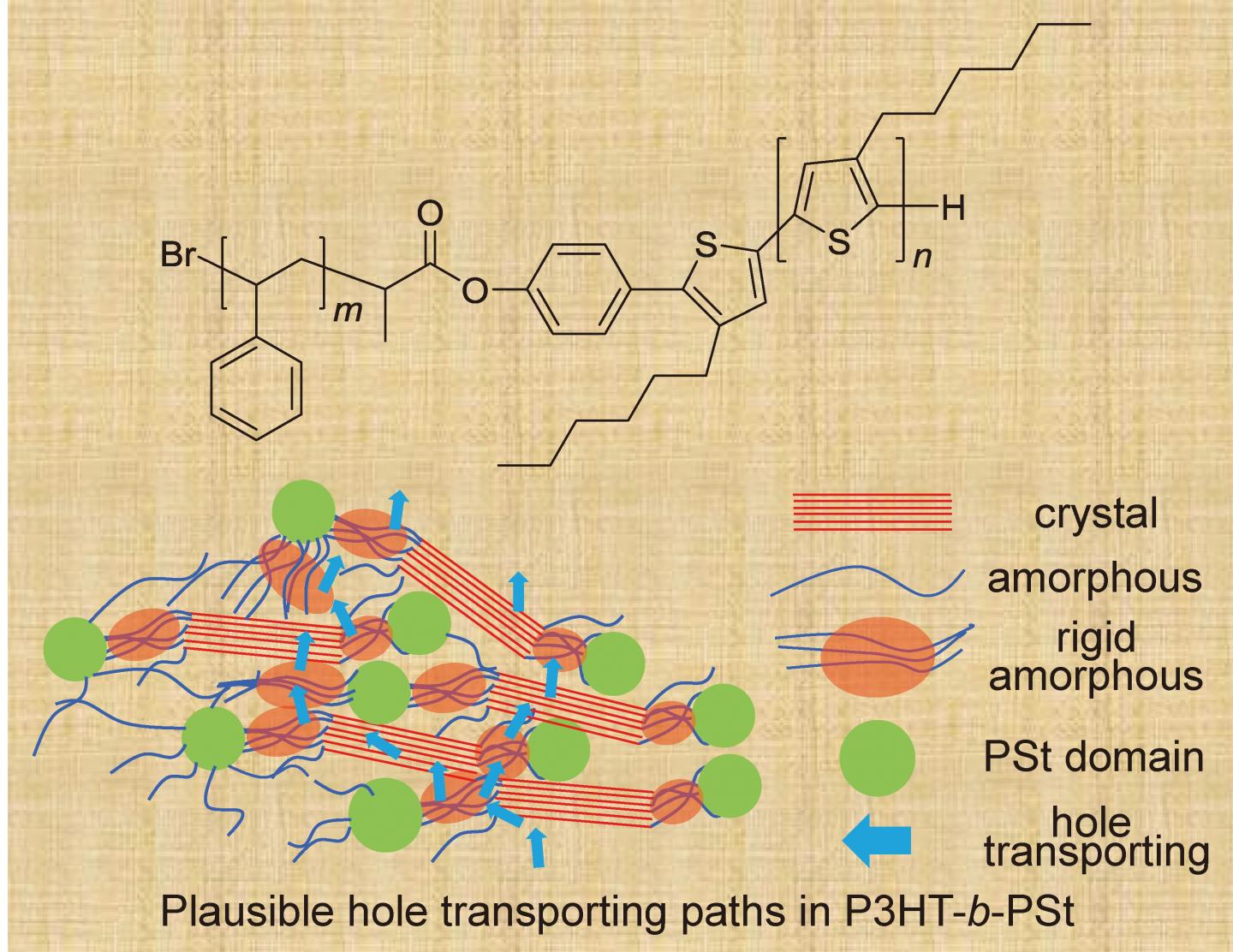
Chemical structure of poly(P3HT)-b-(PSt) and a diagram of Plausible hole transporting paths in P3HT-b-PSt. Credit: Figure adapted with permission from the front cover of Macromol. Chem. Phys. 18/2018. Copyright © 2018, John Wiley and Sons

Researchers have found a way to speed up the electrons in semiconductors, which could lead to improved solar power and transistor use.

A team from the Graduate School of Bio-Applications and Systems Engineering at the Tokyo University of Agriculture and Technology (TUAT) have found a process to speed up the movement of electrons in organic semiconductor films by two-to-three orders of magnitude.

The scientists found that by adding polystyrene, which is commonly known as Styrofoam, they could enhance the semiconducting polymer by enabling the electrons to move from plane to plane at a quicker pace.

This process, called mobility, is how electrons move through electric fields consisting of multiple layers. However, when a molecule is missing an electron, an electron from a different plane can jump or fall and ultimately take its place.

It is generally easy to follow the electron trail in the crystal-based structures through various imaging techniques. However, the clean, defined lines of the crystalline skeleton that intertwine in many semiconducting polymers feature a substantially more difficult-to-define region called the amorphous domain.

“[Electrons] transport in both crystalline and amorphous domains,” Kenji Ogino, a professor at Graduate School of Bio-Applications and Systems Engineering at TUAT, said in a statement. “To improve the total electron mobility, it is necessary to control the nature of the amorphous domain.

“We found that hole mobility extraordinarily improved by the introduction of polystyrene block accompanied by the increase of the ratio of rigid amorphous domain,” he added.

According to the researchers, the way the crystalline domain connects within itself likely occurs most effectively through the rigid amorphous domain. By adding polystyrene, the researchers created a more amorphous domain that is contained by flexible chains of carbons and hydrogen atoms.

The flexible chains provide enough rigidity and control to the amorphous domain to enable the electrons to move two-to-three times quicker than they normally would. Enhanced hole mobility will allow researchers to develop more efficient solar devices.   

“The introduction of a flexible chain in semicrystalline polymers is one of the promising strategies to improve the various functionalities of polymer films by altering the characteristics of the amorphous domain,” Ogino said. “We propose that the rigid amorphous domain plays an important role in the hole transporting process.”

The researchers next plan to examine how the enhanced hole mobility affects other parameters like the chemical composition and position of the structures within the polymer film.

The study was published in Macromolecular Chemistry and Physics.

Related Articles Read More >

‘Self-driving’ lab speeds up research, synthesis of energy materials
Record-breaking, ultrafast devices step to protecting the grid from EMPs
Surprising semiconductor properties revealed with innovative new method
Thermo Scientific Centrios HX offers precise circuit edit solution for fast prototyping
2021 R&D Global Funding Forecast

Need R&D World news in a minute?

We Deliver!
R&D World Enewsletters get you caught up on all the mission critical news you need in research and development. Sign up today.
Enews Signup

R&D World Digital Issues

February 2020 issue

Browse the most current issue of R&D World and back issues in an easy to use high quality format. Clip, share and download with the leading R& magazine today.

Research & Development World
  • Subscribe to R&D World Magazine
  • Enews Sign Up
  • Contact Us
  • About Us
  • Drug Discovery & Development
  • Pharmaceutical Processing
  • 2022 Global Funding Forecast

Copyright © 2022 WTWH Media LLC. All Rights Reserved. The material on this site may not be reproduced, distributed, transmitted, cached or otherwise used, except with the prior written permission of WTWH Media
Privacy Policy | Advertising | About Us

Search R&D World

  • Home Page
  • Topics
    • Aerospace
    • Archeology
    • Automotive
    • Biotech
    • Chemistry
    • COVID-19
    • Environment
    • Energy
    • Life Science
    • Material Science
    • R&D Market Pulse
    • R&D Management
    • Physics
  • Technology
    • 3D Printing
    • A.I./Robotics
    • Battery Technology
    • Controlled Environments
      • Cleanrooms
      • Graphene
      • Lasers
      • Regulations/Standards
      • Sensors
    • Imaging
    • Nanotechnology
    • Scientific Computing
      • Big Data
      • HPC/Supercomputing
      • Informatics
      • Security
      • Software
    • Semiconductors
  • 2021 R&D 100 Award Winners
    • R&D 100 Awards
    • 2020 Winners
    • Winner Archive
  • Resources
    • Digital Issues
    • Podcasts
    • Subscribe
  • Global Funding Forecast
  • Webinars