Researchers from IMDEA Nanociencia and other European centers have discovered that the combination of graphene with cobalt offers relevant properties in the field of magnetism. This breakthrough sets the stage for the development of new logic devices that can store large data amounts quickly and with reduced energy consumption.
One of the latest technologies for digitally encoding information is spin orbitronics, which not only exploits the charge of the electron (electronics) and its spin (spintronics), but also the interaction of the spin with its orbital motion, offering a multitude of properties that are relevant in magnetism.
This technology is applied in certain materials to generate magnetic configurations that are very stable but which can be controlled and moved quickly with very small electrical currents. The resulting structures are considered very promising for future spin-orbitronic devices, as they provide high processing speed and a high capacity for storing data, with low energy consumption.
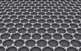
Now, a European team led by the IMDEA Nanociencia Institute has developed a methodology to prepare such a system. It consists of a device made of stacked graphene films (a single atomic graphite layer) placed on ferromagnetic cobalt, arranged in turn on a platinum layer with a certain crystallographic orientation. The details are published in Nano Letters.
The main author of the study, Paolo Perna from IMDEA Nanociencia, explains the advantages of this configuration: “On the one hand, the exceptional properties of graphene make it possible to obtain a homogeneous, flat and protected magnetic layer, which is also atomically perfect. However, what matters most are the two magnetic properties that are achieved: an improvement in the magnetic anisotropy of cobalt (its spines are preferably oriented in a certain direction), and a strong interaction called Dzyaloshinskii-Moriya, which allows the presence of chiral magnetic structures, as they do not overlap with its specular image.”
These chiral magnetic structures of nanometric size are called skyrmions. They are very stable and act as carriers of binary information as they travel through graphene.
“By passing through two electrical contacts, each skyrmion produces a change in the electrical response that can be decoded into zeros and ones,” explains Perna.
“In this way, in the near future, it will be possible to produce spin-orbitronic magnetic devices such as magnetic memories or sensors that are much faster and denser than current ones, and with much lower energy consumption,” the researcher says.
In order to detect the properties, the authors have used combined spectroscopy and microscopy techniques, including some with light at the ALBA synchrotron near Barcelona. Researchers from the Complutense and Autonomous Universities of Madrid, together with the Néel Institute of Grenoble (France), have also participated in the study.
As the basis of the device, the authors have used oxide insulating substrates. In order to obtain high-quality graphene, metallic substrates are usually used in laboratories, but they are very expensive for the industry and, as conductors, they would not allow the electrical insulation of the device with the chip.
“We have proven that it is feasible to prepare high quality magnetic structures based on graphene and on oxide insulating substrates, which can be implemented in current manufacturing processes,” Perna notes.


