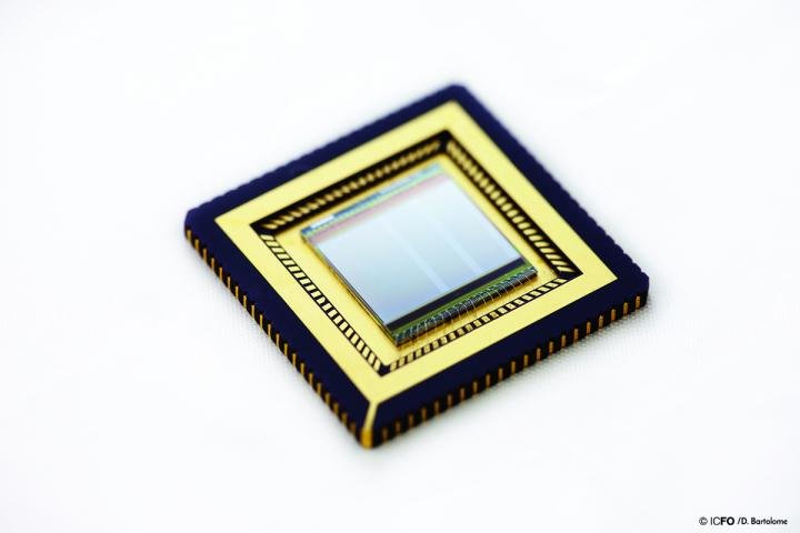
Graphene-quantum dots-CMOS-based sensor for ultraviolet, visible, and infrared. Image: ICFO/ D. Bartolome
Over the past 40 years, microelectronics has advanced by leaps and bounds thanks to silicon and CMOS (Complementary metal-oxide semiconductors) technology, making possible computing, smartphones, compact and low-cost digital cameras, as well as most of the electronic gadgets we rely on today. However, the diversification of this platform into applications other than microcircuits and visible light cameras has been impeded by the difficulty to combine semiconductors other than silicon with CMOS.
This obstacle has now been overcome. ICFO researchers have shown for the first time the monolithic integration of a CMOS integrated circuit with graphene, resulting in a high-resolution image sensor consisting of hundreds of thousands of photodetectors based on graphene and quantum dots (QD). They operated it as a digital camera that is highly sensitive to UV, visible and infrared light at the same time. This has never been achieved before with existing imaging sensors. In general, this demonstration of monolithic integration of graphene with CMOS enables a wide range of optoelectronic applications, such as low-power optical data communications and compact and ultra-sensitive sensing systems.
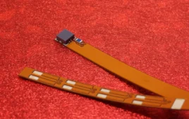
The study was published in Nature Photonics, and highlighted on the front cover image. The work was carried out by ICFO researchers Stijn Goossens, Gabriele Navickaite, Carles Monasterio, Shuchi Gupta, Juan Jose Piqueras, Raul Perez, Gregory Burwell, Ivan Nitkitsky, Tania Lasanta, Teresa Galan, Eric Puma, and led by ICREA Professors Frank Koppens and Gerasimos Konstantatos, in collaboration with the company Graphenea. The graphene-QD image sensor was fabricated by taking PbS colloidal quantum dots, depositing them onto the CVD graphene and subsequently depositing this hybrid system onto a CMOS wafer with image sensor dies and a read-out circuit.
As Stijn Goossens comments, “No complex material processing or growth processes were required to achieve this graphene-quantum dot CMOS image sensor. It proved easy and cheap to fabricate at room temperature and under ambient conditions, which signifies a considerable decrease in production costs. Even more, because of its properties, it can be easily integrated on flexible substrates as well as CMOS-type integrated circuits.”
As ICREA Prof. at ICFO Gerasimos Konstantatos, expert in quantum dot-graphene research comments, “we engineered the QDs to extend to the short infrared range of the spectrum (1100 to 1900nm), to a point where we were able to demonstrate and detect the night glow of the atmosphere on a dark and clear sky enabling passive night vision. This work shows that this class of phototransistors may be the way to go for high sensitivity, low-cost, infrared image sensors operating at room temperature addressing the huge infrared market that is currently thirsty for cheap technologies.”
“The development of this monolithic CMOS-based image sensor represents a milestone for low-cost, high-resolution broadband and hyperspectral imaging systems” ICREA Professor at ICFO Frank Koppens highlights. He assures that “in general, graphene-CMOS technology will enable a vast amount of applications, that range from safety, security, low cost pocket and smartphone cameras, fire control systems, passive night vision and night surveillance cameras, automotive sensor systems, medical imaging applications, food and pharmaceutical inspection to environmental monitoring, to name a few.”
This project is currently incubating in ICFO’s Launchpad. The team is working with the institute’s tech transfer professionals to bring this breakthrough along with its full patent portfolio of imaging and sensing technologies to the market.
This research has been partially supported by the European Graphene Flagship, the European Research Council, the Government of Catalonia, Fundació Cellex, and the Severo Ochoa Excellence program of the Government of Spain.
Source: ICFO