Research & Development World

  • R&D World Home
  • Topics
    • Aerospace
    • Automotive
    • Biotech
    • Careers
    • Chemistry
    • Environment
    • Energy
    • Life Science
    • Material Science
    • R&D Management
    • Physics
  • Technology
    • 3D Printing
    • A.I./Robotics
    • Software
    • Battery Technology
    • Controlled Environments
      • Cleanrooms
      • Graphene
      • Lasers
      • Regulations/Standards
      • Sensors
    • Imaging
    • Nanotechnology
    • Scientific Computing
      • Big Data
      • HPC/Supercomputing
      • Informatics
      • Security
    • Semiconductors
  • R&D Market Pulse
  • R&D 100
    • 2025 R&D 100 Award Winners
    • 2025 Professional Award Winners
    • 2025 Special Recognition Winners
    • R&D 100 Awards Event
    • R&D 100 Submissions
    • Winner Archive
  • Resources
    • Research Reports
    • Digital Issues
    • Educational Assets
    • Subscribe
    • Video
    • Webinars
    • PharmSci360
    • Content submission guidelines for R&D World
  • Global Funding Forecast
  • Top Labs
  • Advertise
  • SUBSCRIBE

Inkjet Printers Can Produce Cheap Micro-Waveguides For Optical Computers

By ITMO University | November 20, 2018

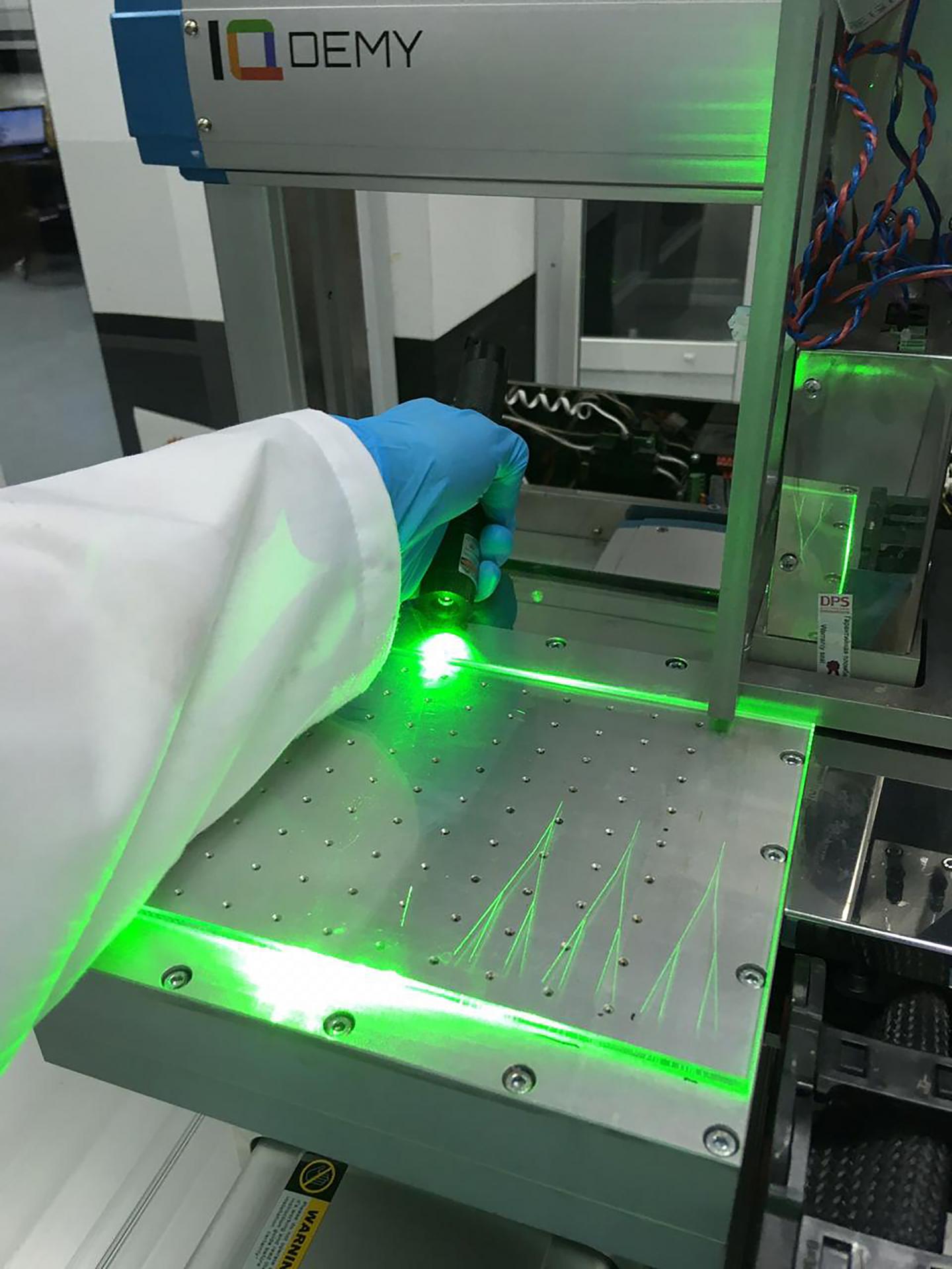
Photo of the samples made by industrial equipment. Credit: ITMO University

Scientists from ITMO University have proposed a new technology for creating optical micro-waveguides using inkjet printing. Using this method it is possible to quickly create waveguides with the necessary parameters without expensive equipment and complex procedures. The new technology is optimized for the production of optical elements on an industrial scale. The results are published in Advanced Optical Materials on 20th November 2018.

Today, optical fiber is widely used in communication. Many people know that it can transmit a signal over long distances with minimal losses providing, for example, high-speed Internet. However, as devices become smaller and smaller, scientists and engineers try to create an analogue of fiber on a microscale. Such devices are called waveguides. They are necessary for new computers on an optical basis in order to ensure efficient signal transmission and processing.

Most researchers now suggest complex and expensive technologies for creating waveguides: for example, laser ablation or photolithography. These are time-consuming procedures requiring complex equipment, rare materials and additional sample processing. However, scientists from ITMO University offer an alternative method for creating optical micro-waveguides, based on a common inkjet technology.

Waveguide printing begins with the preparation of special ink. Its main ingredient is a suspended solution, or sol, of titanium dioxide nanoparticles. Such a material was chosen due to the high refractive index, which is necessary for the waveguide to effectively conduct the signal. In order to achieve suitable ink parameters, the scientists selected the solvents, the concentration of the main component and the surfactants. After that the ink is filled in an inkjet printer, which applies the material according to a given geometry on a clean glass substrate.

“The feature of our work is that we explained the choice of material, working wavelength and waveguide geometry, instead of simple description of properties and methods. However, the main advantage is a simple and cheap method suitable for industry. This work was initially aimed at practically applicable result, and now we conducted the first industrial tests of our technology together with “IQDemy” company. The results confirmed that the method can be adapted without losing the waveguides quality”, comments Anastasia Klestova, member of SCAMT Laboratory of ITMO University.

Currently, scientists work not only on the industrial adaptation of waveguide inkjet printing. The near plans of the laboratory include applying inkjet printing for the creation of other elements necessary for processing the optical signal.

“It is obvious that the creation of elements of data storage and transmission of data based on the photons movement control is the basic technology for future computers. The most difficult part for the engineering of such devices is the creation of efficient signal transport lines. Our solution, actually, removes all the major limitations in this area and I have no doubt that soon we will see photon computing devices with waveguides created with our method,” notes Alexander Vinogradov, researcher at the SCAMT Laboratory of ITMO University.


Related Articles Read More >

Speaker Giving a Talk at Business Meeting. Audience in the conference hall. Business and Entrepreneurship. Panoramic composition suitable for banners.
BioPharma Supply Chain & Logistics Nexus returns to San Diego in November
How Cypris evolved from selling patent reports to agentic R&D intelligence
New video series: Travel for engineers
Advanced Manufacturing and Process Innovation Special Report: When you can’t hire, you automate
rd newsletter
EXPAND YOUR KNOWLEDGE AND STAY CONNECTED
Get the latest info on technologies, trends, and strategies in Research & Development.

R&D World Digital Issues

Fall 2025 issue

Browse the most current issue of R&D World and back issues in an easy to use high quality format. Clip, share and download with the leading R&D magazine today.

R&D 100 Awards
Research & Development World
  • Subscribe to R&D World Magazine
  • Sign up for R&D World’s newsletter
  • Contact Us
  • About Us
  • Drug Discovery & Development
  • Pharmaceutical Processing
  • Global Funding Forecast

Copyright © 2026 Arrowfly LLC. All Rights Reserved. The material on this site may not be reproduced, distributed, transmitted, cached or otherwise used, except with the prior written permission of Arrowfly
Privacy Policy | Advertising | About Us

Search R&D World

  • R&D World Home
  • Topics
    • Aerospace
    • Automotive
    • Biotech
    • Careers
    • Chemistry
    • Environment
    • Energy
    • Life Science
    • Material Science
    • R&D Management
    • Physics
  • Technology
    • 3D Printing
    • A.I./Robotics
    • Software
    • Battery Technology
    • Controlled Environments
      • Cleanrooms
      • Graphene
      • Lasers
      • Regulations/Standards
      • Sensors
    • Imaging
    • Nanotechnology
    • Scientific Computing
      • Big Data
      • HPC/Supercomputing
      • Informatics
      • Security
    • Semiconductors
  • R&D Market Pulse
  • R&D 100
    • 2025 R&D 100 Award Winners
    • 2025 Professional Award Winners
    • 2025 Special Recognition Winners
    • R&D 100 Awards Event
    • R&D 100 Submissions
    • Winner Archive
  • Resources
    • Research Reports
    • Digital Issues
    • Educational Assets
    • Subscribe
    • Video
    • Webinars
    • PharmSci360
    • Content submission guidelines for R&D World
  • Global Funding Forecast
  • Top Labs
  • Advertise
  • SUBSCRIBE