A small rectangle of pink glass, about the size of a postage stamp, sits on Professor Amy Shen’s desk. Despite its outwardly modest appearance, this little glass slide has the potential to revolutionize a wide range of processes, from monitoring food quality to diagnosing diseases.
The slide is made of a “nanoplasmonic” material — its surface is coated in millions of gold nanostructures, each just a few billionths of a square meter in size. Plasmonic materials absorb and scatter light in interesting ways, giving them unique sensing properties. Nanoplasmonic materials have attracted the attention of biologists, chemists, physicists and material scientists, with possible uses in a diverse array of fields, such as biosensing, data storage, light generation, and solar cells.
In several recent papers, Shen and colleagues at the Micro/Bio/Nanofluidics Unit at the Okinawa Institute of Science and Technology (OIST), described their creation of a new biosensing material that can be used to monitor processes in living cells.
“One of the major goals of nanoplasmonics is to search for better ways to monitor processes in living cells in real time,” says Shen. Capturing such information can reveal clues about cell behavior, but creating nanomaterials on which cells can survive for long periods of time yet don’t interfere with the cellular processes being measured is a challenge, she explains.
One of the team’s new biosensors is made from a nanoplasmonic material that is able to accommodate a large number of cells on a single substrate and to monitor cell proliferation, a fundamental process involving cell growth and division, in real time. Seeing this process in action can reveal important insights into the health and functions of cells and tissues.
Researchers in OIST’s Micro/Bio/Nanofluidics Unit described the sensor in a study recently published in the journal Advanced Biosystems.
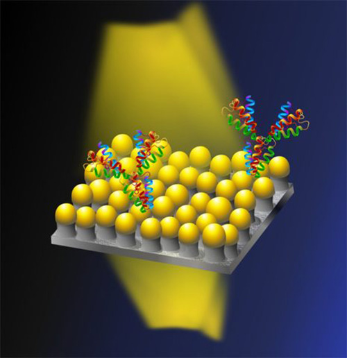
Using their innovative printing technique, the Micro/Bio/Nanofluidics Unit at OIST has developed a nanoplasmonic material containing millions of mushroom-like structures covered with a uniform layer of biomolecules.
The most attractive feature of the material is that it allows cells to survive over long time periods. “Usually, when you put live cells on a nanomaterial, that material is toxic and it kills the cells,” says Dr. Nikhil Bhalla, a postdoctoral researcher at OIST and first author of the paper. “However, using our material, cells survived for over seven days.” The nanoplasmonic material is also highly sensitive: It can detect an increase in cells as small as 16 in 1,000 cells.
The material looks just like an ordinary pieces of glass. However, the surface is coated in tiny nanoplasmonic mushroom-like structures, known as nanomushrooms, with stems of silicon dioxide and caps of gold. Together, these form a biosensor capable of detecting interactions at the molecular level.
The biosensor works by using the nanomushroom caps as optical antennae. When white light passes through the nanoplasmonic slide, the nanomushrooms absorb and scatter some of the light, changing its properties. The absorbance and scattering of light is determined by the size, shape and material of the nanomaterial and, more importantly, it is also affected by any medium in close proximity to the nanomushroom, such as cells that have been placed on the slide. By measuring how the light has changed once it emerges through the other side of the slide, the researchers can detect and monitor processes occurring on the sensor surface, such as cell division.
“Normally, you have to add labels, such as dyes or molecules, to cells, to be able to count dividing cells,” says Bhalla. “However, with our method, the nanomushrooms can sense them directly.”
This work builds on a new method, developed by scientists at the Micro/Bio/Nanofluidics Unit at OIST, for fabricating nanomushroom biosensors. The technique was published in the journal ACS Applied Materials and Interfaces in December 2017.
Producing large-scale nanoplasmonic materials is challenging because it is difficult to ensure uniformity across the entire material surface. For this reason, biosensors for routine clinical examinations, such as disease testing, are still lacking.
In response to this problem, the OIST researchers developed a novel printing technique to create large-scale nanomushroom biosensors. With their method, they were able to develop a material consisting of approximately one million mushroom-like structures on a 2.5cm by 7.5cm silicon dioxide substrate.
“Our technique is like taking a stamp, covering it with ink made from biological molecules, and printing onto the nanoplasmonic slide,” says Shivani Sathish, a PhD student at OIST and co-author of the paper. The biological molecules increase the sensitivity of the material, meaning it can sense extremely low concentrations of substances, such as antibodies, and thus potentially detect diseases in their earliest stages.
“Using our method, it is possible to create a highly sensitive biosensor that can detect even single molecules,” says Bhalla, first author of the paper.
Plasmonic and nanoplasmonic sensors offer important tools for many fields, from electronics to food production to medicine. For example, in December 2017, second year Ph.D student Ainash Garifullina from the Unit developed a new plasmonic material for monitoring the quality of food products during the manufacturing process. The results were published in the journal Analytical Methods.
Prof. Shen and her unit say that, in the future, nanoplasmonic materials may even be integrated with emerging technologies, such as wireless systems in microfluidic devices, allowing users to take readings remotely and thereby minimizing the risk of contamination.


