Research & Development World

  • R&D World Home
  • Topics
    • Aerospace
    • Automotive
    • Biotech
    • Careers
    • Chemistry
    • Environment
    • Energy
    • Life Science
    • Material Science
    • R&D Management
    • Physics
  • Technology
    • 3D Printing
    • A.I./Robotics
    • Software
    • Battery Technology
    • Controlled Environments
      • Cleanrooms
      • Graphene
      • Lasers
      • Regulations/Standards
      • Sensors
    • Imaging
    • Nanotechnology
    • Scientific Computing
      • Big Data
      • HPC/Supercomputing
      • Informatics
      • Security
    • Semiconductors
  • R&D Market Pulse
  • R&D 100
    • 2026 R&D 100 Award Winners
    • 2026 Professional Award Winners
    • 2026 Special Recognition Winners
    • R&D 100 Awards Event
    • R&D 100 Submissions
    • Winner Archive
  • Resources
    • Research Reports
    • Digital Issues
    • Educational Assets
    • Subscribe
    • Video
    • Webinars
    • PharmSci360
    • Content submission guidelines for R&D World
  • Global Funding Forecast
  • Top Labs
  • Advertise
  • SUBSCRIBE

New Technique Creates Eco-friendly Waterborne Semiconductor Inks

By R&D Editors | November 27, 2017

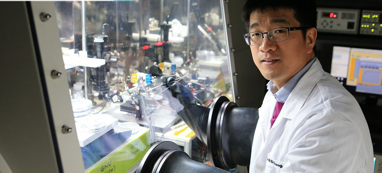
Professor Dae Sung Chung of Energy Science and Engineering in his laboratory at DGIST.

A team of researchers at Daegu Gyeongbuk Institute of Science and Technology (DGIST), led by Professor Dae Sung Chung of Energy Science and Engineering, has developed a technology to produce environmentally friendly water-borne semiconductor inks using surfactant, which is additives that mix substances of different properties and a component of soap.

Polymer semiconductors are carbon compounds showing the electrical properties of semiconductors. It has been highlighted as a next-generation material of wearable smart devices, etc. not only because they are flexible and light in weight, but also they can be processed in a wide area a low cost through the solution process. However, there is an issue that it causes significant environmental pollution as toxic organic solvents are used in the process.

Despite the limitations, the research team has developed a semiconductor surface control technique using surfactants for environmentally friendly semiconductor manufacturing processes that do not use toxic organic solvents and has produced water-borne semiconductor inks.

In the study, the newly developed waterborne semiconductor ink of the research team has small colloidal particles and less surfactant micelles compared to the waterborne semiconductor inks in the previous studies. As a result, it has a relatively flat surface than the conventional waterborne semiconductor inks. The black and white image in the below figure shows the comparison of the surface of the thin film made with the waterborne semiconductor ink developed in this study and conventional one.

According to the research team, the technique is expected to be applied in various electronic devices such as P-type and N-type transistors as well as PN diodes, complementary inverters, photodiodes as high-quality thin films.
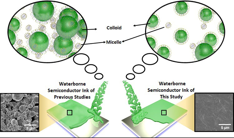
A comparison of the waterborne semiconductor ink of this study and that of the previous studies.

Chung stressed the significance of the study by stating, “This research has fundamentally solved the environmental pollution problem generated during the production of organic semiconductor, which is spotlighted as the core material of wearable electronic devices. We have developed a source technology that can disperse various semiconductor materials into water through the simple chemical modification. We expect that it can be used in various optoelectronic devices ranging from transistors to solar cell, composite circuit, and image sensor.”

This study has been published as the cover thesis of the Energy & Environmental Science, an international journal of energy, on Nov. 8. The study was conducted with the support of Basic Research Support Project (Individual Research) by the Ministry of Science and ICT.


Source: Daegu Gyeongbuk Institute of Science and Technology

Related Articles Read More >

Startup Architect Labs says its AI-designed chip beats NVIDIA’s Jetson Orin Nano
SK Telecom puts SK hynix fabs into an NVIDIA Omniverse twin, following Samsung and TSMC
What Apple’s new CEO could mean for its R&D strategy
Copper is hitting its physical limit with AI. Why NTT thinks photonics is could unblock it.
rd newsletter
EXPAND YOUR KNOWLEDGE AND STAY CONNECTED
Get the latest info on technologies, trends, and strategies in Research & Development.

R&D World Digital Issues

Fall 2025 issue

Browse the most current issue of R&D World and back issues in an easy to use high quality format. Clip, share and download with the leading R&D magazine today.

R&D 100 Awards
Research & Development World
  • Subscribe to R&D World Magazine
  • Sign up for R&D World’s newsletter
  • Contact Us
  • About Us
  • Drug Discovery & Development
  • Pharmaceutical Processing
  • Global Funding Forecast

Copyright © 2026 Arrowfly LLC. All Rights Reserved. The material on this site may not be reproduced, distributed, transmitted, cached or otherwise used, except with the prior written permission of Arrowfly
Privacy Policy | Advertising | About Us

Search R&D World

  • R&D World Home
  • Topics
    • Aerospace
    • Automotive
    • Biotech
    • Careers
    • Chemistry
    • Environment
    • Energy
    • Life Science
    • Material Science
    • R&D Management
    • Physics
  • Technology
    • 3D Printing
    • A.I./Robotics
    • Software
    • Battery Technology
    • Controlled Environments
      • Cleanrooms
      • Graphene
      • Lasers
      • Regulations/Standards
      • Sensors
    • Imaging
    • Nanotechnology
    • Scientific Computing
      • Big Data
      • HPC/Supercomputing
      • Informatics
      • Security
    • Semiconductors
  • R&D Market Pulse
  • R&D 100
    • 2026 R&D 100 Award Winners
    • 2026 Professional Award Winners
    • 2026 Special Recognition Winners
    • R&D 100 Awards Event
    • R&D 100 Submissions
    • Winner Archive
  • Resources
    • Research Reports
    • Digital Issues
    • Educational Assets
    • Subscribe
    • Video
    • Webinars
    • PharmSci360
    • Content submission guidelines for R&D World
  • Global Funding Forecast
  • Top Labs
  • Advertise
  • SUBSCRIBE