Japanese researchers have developed a new method to build large areas of semiconductive material that is just two molecules thick and a total of 4.4 nanometers tall. The films function as thin film transistors, and have potential future applications in flexible electronics or chemical detectors. These thin film transistors are the first example of semiconductive single molecular bilayers created with liquid solution processing, a standard manufacturing process that minimizes costs.
“We want to give electronic devices the features of real cell membranes: flexible, strong, sensitive, and super thin. We found a novel way to design semiconductive single molecular bilayers that allows us to manufacture large surface areas, up to 100 square centimeters (39 square inches). They can function as high performance thin film transistors and could have many applications in the future,” said Assistant Professor Shunto Arai, the first author on the recent research publication.
Professor Tatsuo Hasegawa of the University of Tokyo Department of Applied Physics led the team that built the new film. The breakthrough responsible for their success is a concept called geometric frustration, which uses a molecular shape that makes it difficult for molecules to settle in multiple layers on top of each other.
The film is transparent, but the forces of attraction and repulsion between the molecules create an organized, repeated herringbone pattern when the film is viewed from above through a microscope. The overall molecular structure of the bilayer is highly stable. Researchers believe it should be possible to build the same structure out of different molecules with different functionalities.
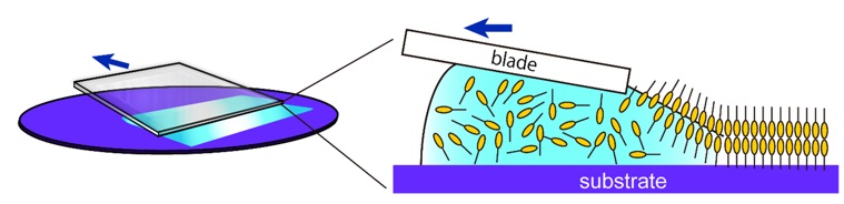
Artist’s representation of the blade coating solution process to produce single molecular bilayer thin film transistors. Liquid molecules are spread by a blade over the production surface at room temperature and standard air pressure in a technique called solution processing. As the liquid dries, the inter-molecular forces cause the molecules to automatically arrange themselves into geometrically frustrated single bilayers just 4.4 nanometers thick. Image: © 2018 Shunto Arai and Tatsuo Hasegawa
The individual molecules used in the current film are divided into two regions: a head and a tail. The head of one molecule stacks on top of another, with their tails pointing in opposite directions so the molecules form a vertical line. These two molecules are surrounded by identical head-to-head pairs of molecules, which all together form a sandwich called a molecular bilayer.
Researchers discovered they could prevent additional bilayers from stacking on top by building the bilayer out of molecules with different length tails, so the surfaces of the bilayer are rough and naturally discourage stacking. This effect of different lengths is referred to as geometric frustration.
Standard methods of creating semiconductive molecular bilayers cannot control the thickness without causing cracks or an irregular surface. The geometric frustration of different length tails has allowed researchers to avoid these pitfalls and build a 10cm by 10cm (3.9 inches by 3.9 inches) square of their film using the common industrial method of solution processing.
The semiconductive properties of the bilayer may give the films applications in flexible electronics or chemical detection.
Semiconductors are able to switch between states that allow electricity to flow (conductors) and states that prevent electricity from flowing (insulators). This on-off switching is what allows transistors to quickly change displayed images, such as a picture on an LCD screen. The single molecular bilayer created by the UTokyo team is much faster than amorphous silicon thin film transistors, a common type of semiconductor currently used in electronics.
The team will continue to investigate the properties of geometrically frustrated single molecular bilayers and potential applications for chemical detection. Collaborators based at the National Institute of Advanced Industrial Science and Technology, the Nippon Kayaku Company Limited, Condensed Matter Research Center, and High Energy Accelerator Research Organization also contributed to the research.
Source: University of Tokyo


