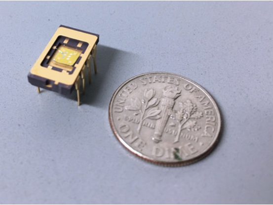
A small integrated circuit rests on a surface next to a time, which is comparable in size A phononic device next to a dime for scale. Credit: Caltech
Scientists have developed microscopic components that could usher in the next generation of sensors, mobile phones and quantum computing.
A Caltech research group has created new versions of the components that make up mobile devices called phononic devices, which have the ability to vibrate extremely fast, moving back and forth up to tens of millions of times per second.
Currently, modern mobile devices are comprised of materials that utilize acoustic waves to filter or delay communication signals. However, current strategies have limited functionalities that prevent further miniaturization of future devices, while constraining the available communication bandwidth.
To develop the improved devices the researchers created 90 nanometer thick silicon nitride drums that they then arranged into grids with different grid patterns containing different properties. The arrangement of the arrays of these drums acts as a tunable filter for signals of different frequencies. The researchers also found that the devices could act like one-way valves for high-frequency waves to keep the signal stronger by reducing interference.
The researchers demonstrated the presence of edge states by characterizing their localization and Dirac cone-like frequency dispersion. The newly produced topological waveguides exhibit robustness to waveguide distortions and pseudospin-dependent transport.
“Wave-guiding through a stable physical channel is strongly desired for reliable information transport in on-chip devices,” the authors write. “However, energy transport in high-frequency mechanical systems, for example based on microscale phononic devices, is particularly sensitive to defects and sharp turns because of back-scattering and losses.
“Two-dimensional topological insulators, first described as quantum spin hall insulators [QSHE] in condensed matter, demonstrated robustness and spin-dependent energy transport along materials’ boundaries and interfaces. Translating these properties in the classical domain offers opportunity for scaling the size of acoustic components to on-chip device levels.”
Recently, photonic systems have demonstrated the use of topological effects for lasing and quantum interfaces. However, acoustic and mechanical topological systems have thus far been realized only in large-scale systems like arrays of pendula, gyroscopic lattices and arrays of steel rods, laser-cut plates, which require external driving systems.
“Topological mechanical metamaterials translate condensed matter phenomena, like non-reciprocity and robustness to defects, in to classical platforms,” the authors write. “At small scales, topological nanoelectromechanical metamaterials [NEMM] can enable the realization of on-chip acoustic components, like unidirectional waveguides and compact delay-lines for mobile devices.”
One of the two studies appeared in Nature Nanotechnology, while the other study was published in Nature.


