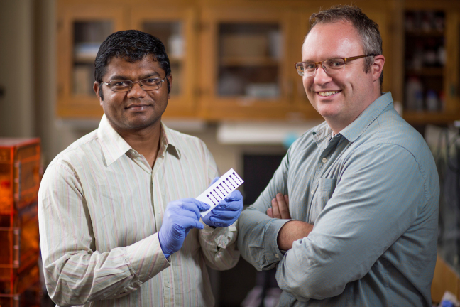
Suprem Das holds graphene electronics printed on a sheet of paper. Das and Jonathan Claussen, right, are using lasers to treat the printed graphene electronics. The process improves conductivity and enables flexible, wearable and low-cost electronics. Image: Christopher Gannon.
The researchers in Jonathan Claussen’s lab at Iowa State University (who like to call themselves nanoengineers) have been looking for ways to use graphene and its amazing properties in their sensors and other technologies.
Graphene is a wonder material: The carbon honeycomb is just an atom thick. It’s great at conducting electricity and heat; it’s strong and stable. But researchers have struggled to move beyond tiny lab samples for studying its material properties to larger pieces for real-world applications.
Recent projects that used inkjet printers to print multi-layer graphene circuits and electrodes had the engineers thinking about using it for flexible, wearable, and low-cost electronics. For example, “Could we make graphene at scales large enough for glucose sensors?” asks Suprem Das, an Iowa State postdoctoral research associate in mechanical engineering and an associate of the U.S. Department of Energy’s Ames Laboratory.
But there were problems with the existing technology. Once printed, the graphene had to be treated to improve electrical conductivity and device performance. That usually meant high temperatures or chemicals — both could degrade flexible or disposable printing surfaces such as plastic films or even paper.
Das and Claussen came up with the idea of using lasers to treat the graphene. Claussen, an Iowa State assistant professor of mechanical engineering and an Ames Laboratory associate, worked with Gary Cheng, an associate professor at Purdue University’s School of Industrial Engineering, to develop and test the idea.
And it worked: They found treating inkjet-printed, multi-layer graphene electric circuits and electrodes with a pulsed-laser process improves electrical conductivity without damaging paper, polymers, or other fragile printing surfaces.
“This creates a way to commercialize and scale-up the manufacturing of graphene,” Claussen says.
The findings are featured on the front cover of the journal Nanoscale’s issue 35. Claussen and Cheng are lead authors and Das is first author. Additional Iowa State co-authors are Allison Cargill, John Hondred and Shaowei Ding, graduate students in mechanical engineering. Additional Purdue co-authors are Qiong Nian and Mojib Saei, graduate students in industrial engineering.
Two major grants are supporting the project and related research: a three-year grant from the National Institute of Food and Agriculture, U.S. Department of Agriculture, under award number 11901762 and a three-year grant from the Roy J. Carver Charitable Trust. Iowa State’s College of Engineering and department of mechanical engineering are also supporting the research.
The Iowa State Research Foundation Inc. has filed for a patent on the technology.
“The breakthrough of this project is transforming the inkjet-printed graphene into a conductive material capable of being used in new applications,” Claussen says.
Those applications could include sensors with biological applications, energy storage systems, electrical conducting components, and even paper-based electronics.
To make all that possible, the engineers developed computer-controlled laser technology that selectively irradiates inkjet-printed graphene oxide. The treatment removes ink binders and reduces graphene oxide to graphene — physically stitching together millions of tiny graphene flakes. The process makes electrical conductivity more than a thousand times better.
“The laser works with a rapid pulse of high-energy photons that do not destroy the graphene or the substrate,” Das says. “They heat locally. They bombard locally. They process locally.”
That localized, laser processing also changes the shape and structure of the printed graphene from a flat surface to one with raised, 3D nanostructures. The engineers say the 3D structures are like tiny petals rising from the surface. The rough and ridged structure increases the electrochemical reactivity of the graphene, making it useful for chemical and biological sensors.
All of that, according to Claussen’s team of nanoengineers, could move graphene to commercial applications.
“This work paves the way for not only paper-based electronics with graphene circuits,” the researchers wrote in their paper, “it enables the creation of low-cost and disposable graphene-based electrochemical electrodes for myriad applications including sensors, biosensors, fuel cells, and (medical) devices.”
Source: Iowa State University