Research & Development World

  • R&D World Home
  • Topics
    • Aerospace
    • Automotive
    • Biotech
    • Careers
    • Chemistry
    • Environment
    • Energy
    • Life Science
    • Material Science
    • R&D Management
    • Physics
  • Technology
    • 3D Printing
    • A.I./Robotics
    • Software
    • Battery Technology
    • Controlled Environments
      • Cleanrooms
      • Graphene
      • Lasers
      • Regulations/Standards
      • Sensors
    • Imaging
    • Nanotechnology
    • Scientific Computing
      • Big Data
      • HPC/Supercomputing
      • Informatics
      • Security
    • Semiconductors
  • R&D Market Pulse
  • R&D 100
    • Call for Nominations: The 2025 R&D 100 Awards
    • R&D 100 Awards Event
    • R&D 100 Submissions
    • Winner Archive
    • Explore the 2024 R&D 100 award winners and finalists
  • Resources
    • Research Reports
    • Digital Issues
    • R&D Index
    • Subscribe
    • Video
    • Webinars
  • Global Funding Forecast
  • Top Labs
  • Advertise
  • SUBSCRIBE

Semiconductor Functions Better when Combined with Graphene

By R&D Editors | February 20, 2015

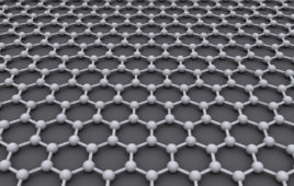
A material made of semiconducting polymer placed on top of graphene conducts electric charge extremely well and may enable new electronic devices. This work was featured on the cover of the journal Advanced Functional Materials. (David Barbero)Graphene – a one-atom-thick sheet of carbon with highly desirable electrical properties, flexibility, and strength – shows great promise for future electronics, advanced solar cells, protective coatings, and other uses, and combining it with other materials could extend its range even further.

Experiments at the Department of Energy’s SLAC National Accelerator Laboratory looked at the properties of materials that combine graphene with a common type of semiconducting polymer. They found that a thin film of the polymer transported electric charge even better when grown on a single layer of graphene than it does when placed on a thin layer of silicon.

“Our results are among the first to measure the charge transport in these materials in the vertical direction – the direction that charge travels in organic photovoltaic devices like solar cells or in light-emitting diodes,” says David Barbero of Umeå University in Sweden, leader of the international research team that performed the experiments at SLAC’s Stanford Synchrotron Radiation Lightsource (SSRL), a DOE Office of Science User Facility. “The result was somewhat expected, because graphene and silicon have different crystalline structures and electrical properties.”

But the team also discovered something very unexpected, he says.

Although it was widely believed that a thinner polymer film should enable electrons to travel faster and more efficiently than a thicker film, Barbero and his team discovered that a polymer film about 50 nanometers thick conducted charge about 50 times better when deposited on graphene than the same film about 10 nanometers thick.

The team concluded that the thicker film’s structure, which consists of a mosaic of crystallites oriented at different angles, likely forms a continuous pathway of interconnected crystals. This, they theorize, allows for easier charge transport than in a regular thin film, whose thin, plate-like crystal structures are oriented parallel to the graphene layer.

Studies conducted at the Stanford Synchrotron Radiation Lightsource revealed that when deposited atop graphene, a thicker polymer film (top) conducted charge significantly better than a thinner polymer film (bottom). This is likely because the orientation of the polymer crystallites within the thick film allows the formation of a continuous pathway for the charge to flow. (David Barbero)By better controlling the thickness and crystalline structure of the semiconducting film, it may be possible to design even more efficient graphene-based organic electronic devices.

“The fields most likely to benefit from this work are probably next-generation photovoltaic devices and flexible electronic devices,” says Barbero. “Because graphene is thin, lightweight, and flexible, there are a number of potential applications.”

Release Date: February 18, 2015
Source: SLAC


Related Articles Read More >

The emerging materials shaping next-generation semiconductor electronics
24 R&D trends that redefined 2024
Graphene-based flowmeter sensor measures nano-rate fluid flows, Part 3: The sensor
Graphene-based flowmeter sensor measures nano-rate fluid flows, Part 2: The graphene context
rd newsletter
EXPAND YOUR KNOWLEDGE AND STAY CONNECTED
Get the latest info on technologies, trends, and strategies in Research & Development.
RD 25 Power Index

R&D World Digital Issues

Fall 2024 issue

Browse the most current issue of R&D World and back issues in an easy to use high quality format. Clip, share and download with the leading R&D magazine today.

Research & Development World
  • Subscribe to R&D World Magazine
  • Enews Sign Up
  • Contact Us
  • About Us
  • Drug Discovery & Development
  • Pharmaceutical Processing
  • Global Funding Forecast

Copyright © 2025 WTWH Media LLC. All Rights Reserved. The material on this site may not be reproduced, distributed, transmitted, cached or otherwise used, except with the prior written permission of WTWH Media
Privacy Policy | Advertising | About Us

Search R&D World

  • R&D World Home
  • Topics
    • Aerospace
    • Automotive
    • Biotech
    • Careers
    • Chemistry
    • Environment
    • Energy
    • Life Science
    • Material Science
    • R&D Management
    • Physics
  • Technology
    • 3D Printing
    • A.I./Robotics
    • Software
    • Battery Technology
    • Controlled Environments
      • Cleanrooms
      • Graphene
      • Lasers
      • Regulations/Standards
      • Sensors
    • Imaging
    • Nanotechnology
    • Scientific Computing
      • Big Data
      • HPC/Supercomputing
      • Informatics
      • Security
    • Semiconductors
  • R&D Market Pulse
  • R&D 100
    • Call for Nominations: The 2025 R&D 100 Awards
    • R&D 100 Awards Event
    • R&D 100 Submissions
    • Winner Archive
    • Explore the 2024 R&D 100 award winners and finalists
  • Resources
    • Research Reports
    • Digital Issues
    • R&D Index
    • Subscribe
    • Video
    • Webinars
  • Global Funding Forecast
  • Top Labs
  • Advertise
  • SUBSCRIBE