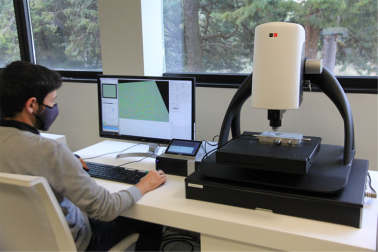
The Linkam LTS420 – Sensofar’s S neox system with Linnik in use in the lab
Sensofar, a technology company specializing in the field of non-contact surface metrology, has developed a new technique for characterizing the evolution of a sample’s surface topography with temperature using the S neox 3D optical profiler and Linnik interferometer coupled with Linkam’s LTS420 temperature-controlled chamber. The technique has been used to successfully map the changes in roughness and waviness of silicon wafers at temperatures up to 380° C (716° F).
Optical profilometry is a rapid, non-destructive and non-contact surface metrology technique, which is used to establish the surface morphology, step heights and surface roughness of materials. It has a wide range of applications across many fields of research, including analyzing the surface texture of paints and coatings, analyzing micro-cracks and scratches and creating wear profiles for structured materials including micro-electronics, and characterization of textured or embossed nanometer-scale semiconducting components, such as silicon wafers.
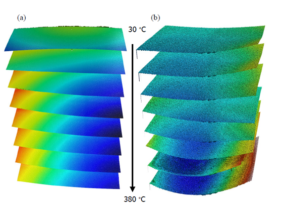
Stacked 4D view of the topographies extracted from two samples corresponding to different chip designs from silicon wafers (a) sample A and (b) sample B for visual comparison of the experimented bow change when samples go from 30º C to 380º C.
Historically, it has been difficult to conduct temperature-controlled optical profilometry experiments due to imaging issues caused by changes in spherical aberration with temperature of both the front lens of the objective and the quartz window of the LTS420 stage.
By using Sensofar’s new Linnik interferometer lens system with the S neox 3D optical profiler, in combination with Linkam’s LTS420 precision temperature control chamber, spherical aberration issues are resolved, enabling the accurate measurement of 3D topographic profiles of nanoscale materials at a wide range of temperatures.
,“In a recent experiment using the new technique, we were able to observe the changes in topography of silicon wafers as they evolve with temperature from 20° C (68° F) up to 380° C (716° F). This is critical information for silicon wafer producers and users, so that they can optimize their process, improve semiconductor properties and wafer durability. The Linkam LTS420 chamber and T96 temperature controller are key components in our experimental set-up and enable us to ramp and control the temperature between -195° and 420° C (-319° and 788° F) to a precision of 0.01° C (32.018° F),” said David Páez, Sensofar sales support specialist.
“We have provided precise temperature and environmental control to a wide range of techniques, from microscopy to X-ray analysis, for decades. This collaboration highlights the important role of temperature control in contributing to innovative approaches to material characterization. We are extremely pleased to be able to offer a solution for temperature-controlled profilometry thanks to Sensofar’s Linnik interferometer, and we look forward to seeing how this new technique helps researchers across many scientific fields to advance their research and knowledge,” said Robert Gurney, Linkam’s application specialist.
Sensofar’s 5th generation S neox 3D optical profiler is the fastest scanning confocal profilometer on the market. It is easy to use and has some key advantages over previous models. The bridge design offers increased stability, and the sensor head uses improved algorithms to produce the fastest system on the market with no moving parts and, therefore, minimum service requirements or need for extensive calibration. The addition of the Linnik interferometer and Linkam LTS420 enables temperature control < -195° C (383° F) to 420° C (788° F). Different brightfield objectives are compatible with the Linnik configuration, offering working distances up to 37 mm and magnifications up to 100x for applications that require high lateral resolution.
Linkam’s LTS420 is an easy to use and very versatile heating and freezing stage. The stage consists of a large area temperature-controlled element with a sensor embedded close to the surface for accurate temperature measurements in the range of < -195° C to 420° C (when used with the LNP96 cooling pump). The sample is easily mounted on a standard microscope slide in direct contact with the heating element and can be manipulated 15 mm in both X and Y directions. The sample chamber is gas tight and has valves to allow atmospheric composition control, and there are options for humidity and electrical probes.
For more information, visit linkam.co.uk


Tell Us What You Think!