Scientists are experimenting with narrow strips of graphene, called nanoribbons, in hopes of making cool new electronic devices, but University of California, Berkeley scientists have discovered another possible role for them: as nanoscale electron traps with potential applications in quantum computers.
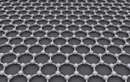
Graphene, a sheet of carbon atoms arranged in a rigid, honeycomb lattice resembling chicken wire, has interesting electronic properties of its own. But when scientists cut off a strip less than about 5 nanometers in width — less than one ten-thousandth the width of a human hair — the graphene nanoribbon takes on new quantum properties, making it a potential alternative to silicon semiconductors.
UC Berkeley theoretician Steven Louie, a professor of physics, predicted last year that joining two different types of nanoribbons could yield a unique material, one that immobilizes single electrons at the junction between ribbon segments.
In order to accomplish this, however, the electron “topology” of the two nanoribbon pieces must be different. Topology here refers to the shape that propagating electron states adopt as they move quantum mechanically through a nanoribbon, a subtle property that had been ignored in graphene nanoribbons until Louie’s prediction.
Two of Louie’s colleagues, chemist Felix Fischer and physicist Michael Crommie, became excited by his idea and the potential applications of trapping electrons in nanoribbons and teamed up to test the prediction. Together they were able to experimentally demonstrate that junctions of nanoribbons having the proper topology are occupied by individual localized electrons.
A nanoribbon made according to Louie’s recipe with alternating ribbon strips of different widths, forming a nanoribbon superlattice, produces a conga line of electrons that interact quantum mechanically. Depending on the strips’ distance apart, the new hybrid nanoribbon is either a metal, a semiconductor or a chain of qubits, the basic elements of a quantum computer.
“This gives us a new way to control the electronic and magnetic properties of graphene nanoribbons,” says Crommie, a UC Berkeley professor of physics. “We spent years changing the properties of nanoribbons using more conventional methods, but playing with their topology gives us a powerful new way to modify the fundamental properties of nanoribbons that we never suspected existed until now.”

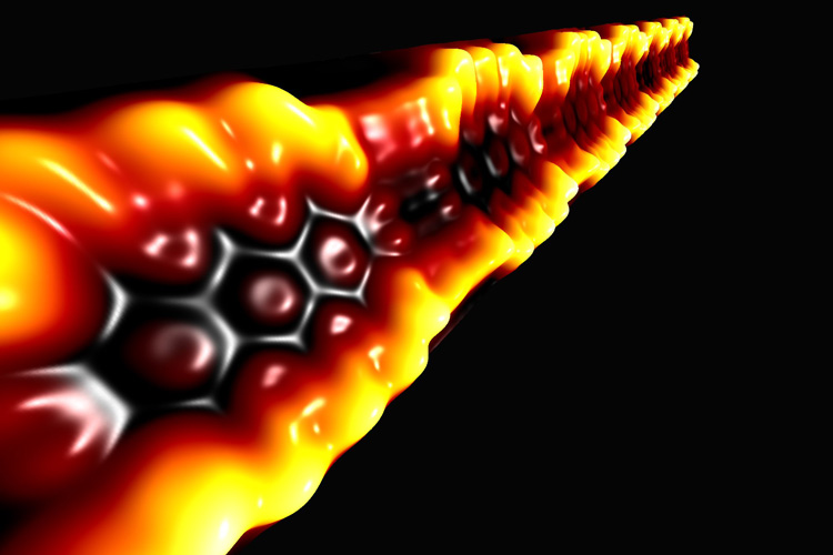
Scanning tunneling microscope image of a topological nanoribbon superlattice. Electrons are trapped at the interfaces between wide ribbon segments (which are topologically non-trivial) and narrow ribbon segments (which are topologically trivial). The wide segments are 9 carbon atoms across (1.65 nanometers) while the narrow segments are only 7 carbon atoms across (1.40 nanometers).
Louie’s theory implies that nanoribbons are topological insulators: unusual materials that are insulators, that is, non-conducting in the interior, but metallic conductors along their surface. The 2016 Nobel Prize in Physics was awarded to three scientists who first used the mathematical principles of topology to explain strange, quantum states of matter, now classified as topological materials.
Three-dimensional topological insulators conduct electricity along their sides, sheets of 2D topological insulators conduct electricity along their edges, and these new 1D nanoribbon topological insulators have the equivalent of zero-dimensional (0D) metals at their edges, with the caveat that a single 0D electron at a ribbon junction is confined in all directions and can’t move anywhere. If another electron is similarly trapped nearby, however, the two can tunnel along the nanoribbon and meet up via the rules of quantum mechanics. And the spins of adjacent electrons, if spaced just right, should become entangled so that tweaking one affects the others, a feature that is essential for a quantum computer.
The synthesis of the hybrid nanoribbons was a difficult feat, said Fischer, a UC Berkeley professor of chemistry. While theoreticians can predict the structure of many topological insulators, that doesn’t mean that they can be synthesized in the real world.
“Here you have a very simple recipe for how to create topological states in a material that is very accessible,” Fischer says. “It is just organic chemistry. The synthesis is not trivial, granted, but we can do it. This is a breakthrough in that we can now start thinking about how to use this to achieve new, unprecedented electronic structures.”
The researchers will report their synthesis, theory and analysis in the Aug. 9 issue of the journal Nature. Louie, Fischer and Crommie are also faculty scientists at Lawrence Berkeley National Laboratory.
Louie, who specializes in the quantum theory of unusual forms of matter, from superconductors to nanostructures, authored a 2017 paper that described how to make graphene nanoribbon junctions that take advantage of the theoretical discovery that nanoribbons are 1D topological insulators. His recipe required taking so-called topologically trivial nanoribbons and pairing them with topologically non-trivial nanoribbons, where Louie explained how to tell the difference between the two by looking at the shape of the quantum mechanical states that are adopted by electrons in the ribbons.
Fischer, who specializes in synthesizing and characterizing unusual nanomolecules, discovered a new way to make atomically precise nanoribbon structures that would exhibit these properties from complex carbon compounds based on anthracene.
Working side by side, Fischer’s and Crommie’s research teams then built the nanoribbons on top of a gold catalyst heated inside a vacuum chamber, and Crommie’s team used a scanning tunneling microscope to confirm the electronic structure of the nanoribbon. It perfectly matched Louie’s theory and calculations. The hybrid nanoribbons they made had between 50 and 100 junctions, each occupied by an individual electron able to quantum mechanically interact with its neighbors.
“When you heat the building blocks, you get a patchwork quilt of molecules knitted together into this beautiful nanoribbon,” Crommie says. “But because the different molecules can have different structures, the nanoribbon can be designed to have interesting new properties.”
Fischer said that the length of each segment of nanoribbon can be varied to change the distance between trapped electrons, thus changing how they interact quantum mechanically. When close together the electrons interact strongly and split into two quantum states (bonding and anti-bonding) whose properties can be controlled, allowing the fabrication of new 1D metals and insulators. When the trapped electrons are slightly more separated, however, they act like small, quantum magnets (spins) that can be entangled and are ideal for quantum computing.
“This provides us with a completely new system that alleviates some of the problems expected for future quantum computers, such as how to easily mass-produce highly precise quantum dots with engineered entanglement that can be incorporated into electronic devices in a straightforward way,” Fischer says.
Co-lead authors of the paper are Daniel Rizzo and Ting Cao from the Department of Physics and Gregory Veber from the Department of Chemistry, along with their colleagues Christopher Bronner, Ting Chen, Fangzhou Zhao and Henry Rodriguez. Fischer and Crommie are both members of the Kavli Energy NanoSciences Institute at UC Berkeley and Berkeley Lab.
The research was supported by the Office of Naval Research, Department of Energy, Center for Energy Efficient Electronics Science, and National Science Foundation.
Source: UC Berkeley


