In the quest to realize artificial photosynthesis to convert sunlight, water, and carbon dioxide into fuel — just as plants do — researchers need to not only identify materials to efficiently perform photoelectrochemical water splitting, but also to understand why a certain material may or may not work. Now scientists at Lawrence Berkeley National Laboratory (Berkeley Lab) have pioneered a technique that uses nanoscale imaging to understand how local, nanoscale properties can affect a material’s macroscopic performance.
Their study, “Nanoscale Imaging of Charge Carrier Transport in Water Splitting Anodes,” has just been published in Nature Communications. The lead researchers were Johanna Eichhorn and Francesca Toma of Berkeley Lab’s Chemical Sciences Division.
“This technique correlates the material’s morphology to its functionality, and gives insights on the charge transport mechanism, or how the charges move inside the material, at the nanoscale,” says Toma, who is also a researcher in the Joint Center for Artificial Photosynthesis, a Department of Energy Innovation Hub.
Artificial photosynthesis seeks to produce energy-dense fuel using only sunlight, water, and carbon dioxide as inputs. The advantage of such an approach is that it does not compete against food stocks and would produce no or low greenhouse gas emissions. A photoelectrochemical water splitting system requires specialized semiconductors that use sunlight to split water molecules into hydrogen and oxygen.
Bismuth vanadate has been identified as a promising material for a photoanode, which provides charges to oxidize water in a photoelectrochemical cell. “This material is a case example in which efficiency should be theoretically good, but in experimental tests you actually observe very poor efficiency,” Eichhorn says. “The reasons for that are not completely understood.”
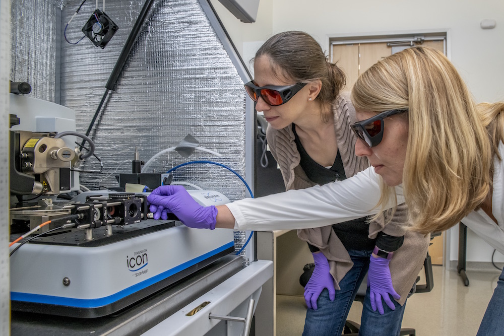
Berkeley Lab researchers Francesca Toma (left) and Johanna Eichhorn used a photoconductive atomic force microscope to better understand materials for artificial photosynthesis. Image: Marilyn Chung/Berkeley Lab
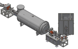
The researchers used photoconductive atomic force microscopy to map the current at every point of the sample with high spatial resolution. This technique has already been used to analyze local charge transport and optoelectronic properties of solar cell materials but is not known to have been used to understand the charge carrier transport limitations at the nanoscale in photoelectrochemical materials.
Eichhorn and Toma worked with scientists at the Molecular Foundry, a nanoscale science research facility at Berkeley Lab, on these measurements through the Foundry’s user program. They found that there were differences in performance related to the nanoscale morphology of the material.
“We discovered that the way charges are utilized is not homogeneous over the whole sample, but rather, there’s heterogeneity,” Eichhorn said. “Those differences in performance may account for its macroscopic performance — the overall output of the sample — when we perform water splitting.”
To understand this characterization, Toma gives the example of a solar panel. “Let’s say the panel has 22 percent efficiency,” she says. “But can you tell at the nanoscale, at each point in the panel, that it will give you 22 percent efficiency? This technique enables you to say, yes or no, specifically for photoelectrochemical materials. If the answer is no, it means there are less active spots on your material. In the best case it just decreases your total efficiency, but if there are more complex processes, your efficiency can be decreased by a lot.”
The improved understanding of how the bismuth vanadate is working will also allow researchers to synthesize new materials that may be able to drive the same reaction more efficiently. This study builds on previous research by Toma and others, in which she was able to analyze and predict the mechanism that defines (photo)chemical stability of a photoelectrochemical material.
Toma says these results put scientists much closer to achieving efficient artificial photosynthesis. “Now we know how to measure local photocurrent in these materials, which have very low conductivity,” she said. “The next step is to put all of this in a liquid electrolyte and do exactly the same thing. We have the tools. Now we know how to interpret the results, and how to analyze them, which is an important first step for moving forward.”
Other co-authors of the study were Christoph Kastl, Jason Cooper, Adam Schwartzberg, and Ian Sharp (now at the Technical University of Munich) of Berkeley Lab; and Dominik Ziegler of Scuba Probe Technologies, a startup company and Molecular Foundry user. The research was funded by Berkeley Lab’s Laboratory Directed Research and Development program (LDRD). The Molecular Foundry is a Department of Energy Office of Science User Facility.
Source: Berkeley Lab