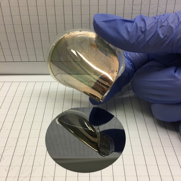
An example of a gold foil peeled from single crystal silicon.Reprinted with permission from Naveen Mahenderkar et al., Science [355]:[1203] (2017)
Some day, your smartphone might completely conform to your wrist, and when it does, it might be covered in pure gold, thanks to researchers at Missouri University of Science and Technology.
Writing in the March 17 issue of the journal Science, the Missouri S&T researchers say they have developed a way to “grow” thin layers of gold on single crystal wafers of silicon, remove the gold foils, and use them as substrates on which to grow other electronic materials.
The research team’s discovery could revolutionize wearable or “flexible” technology research, greatly improving the versatility of such electronics in the future.
According to lead researcher Dr. Jay A. Switzer, the majority of research into wearable technology has been done using polymer substrates, or substrates made up of multiple crystals. “And then they put some typically organic semiconductor on there that ends up being flexible, but you lose the order that (silicon) has,” says Switzer, Donald L. Castleman/FCR Endowed Professor of Discovery in Chemistry at S&T.
Because the polymer substrates are made up of multiple crystals, they have what are called grain boundaries, says Switzer. These grain boundaries can greatly limit the performance of an electronic device.
“Say you’re making a solar cell or an LED,” he says. “In a semiconductor, you have electrons and you have holes, which are the opposite of electrons. They can combine at grain boundaries and give off heat. And then you end up losing the light that you get out of an LED, or the current or voltage that you might get out of a solar cell.”
Most electronics on the market are made of silicon because it’s “relatively cheap, but also highly ordered,” Switzer says.
“99.99 percent of electronics are made out of silicon, and there’s a reason – it works great,” he says. “It’s a single crystal, and the atoms are perfectly aligned. But, when you have a single crystal like that, typically, it’s not flexible.”
By starting with single crystal silicon and growing gold foils on it, Switzer is able to keep the high order of silicon on the foil. But because the foil is gold, it’s also highly durable and flexible.
“We bent it 4,000 times, and basically the resistance didn’t change,” he says.
The gold foils are also essentially transparent because they are so thin. According to Switzer, his team has peeled foils as thin as seven nanometers.
Switzer says the challenge his research team faced was not in growing gold on the single crystal silicon, but getting it to peel off as such a thin layer of foil. Gold typically bonds very well to silicon.
“So we came up with this trick where we could photo-electrochemically oxidize the silicon,” Switzer says. “And the gold just slides off.”
Photoelectrochemical oxidation is the process by which light enables a semiconductor material, in this case silicon, to promote a catalytic oxidation reaction.
Switzer says thousands of gold foils—or foils of any number of other metals—can be made from a single crystal wafer of silicon.
The research team’s discovery can be considered a “happy accident.” Switzer says they were looking for a cheap way to make single crystals when they discovered this process.
“This is something that I think a lot of people who are interested in working with highly ordered materials like single crystals would appreciate making really easily,” he says. “Besides making flexible devices, it’s just going to open up a field for anybody who wants to work with single crystals.”
The research team included Naveen Kumar Mahenderkar, a Ph.D. candidate in materials science and engineering; Qingzhi Chen and Ying Chau Liu, both Ph.D. candidates in chemistry; Alexander Duchild, an undergraduate chemistry student; Seth Hofheins, a student at Rolla High School; and Dr. Eric Chason, professor of engineering at Brown University.


