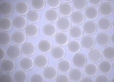
Similar to carbon, silicon forms two dimensional networks that are only one atomic layer thick. Like graphene these layers possess extraordinary optoelectrical properties. Embedding them in a polymer, scientists at the Technical University of Munich (TUM) have developed a stable composite material which can be processed with standard polymer technology. Source: Tobias Helbich / TUM
Silicon nanosheets are thin, two-dimensional layers with exceptional optoelectronic properties very similar to those of graphene. Albeit, the nanosheets are less stable. Now researchers at the Technical University of Munich (TUM) have, for the first time ever, produced a composite material combining silicon nanosheets and a polymer that is both UV-resistant and easy to process. This brings the scientists a significant step closer to industrial applications like flexible displays and photosensors.
Similar to carbon, silicon forms two dimensional networks that are only one atomic layer thick. Like graphene, for whose discovery Andre Geim and Konstantin Novoselov received the Nobel Prize in 2010, these layers possess extraordinary optoelectrical properties. Silicon nanosheets might thus find application in nanoelectronics, for example in flexible displays, field-effect transistors and photodetectors. With its ability to store lithium ions, it is also under consideration as an anode material in rechargeable lithium batteries.
“Silicon nanosheets are particularly interesting because today’s information technology builds on silicon and, unlike with graphene, the basic material does not need to be exchanged,” explains Tobias Helbich from the WACKER Chair for Macromolecular Chemistry at TUM. “However, the nanosheets themselves are very delicate and quickly disintegrate when exposed to UV light, which has significantly limited their application thus far.”
Polymer and nanosheets – the best of both worlds in one
Now Helbich, in collaboration with Professor Bernhard Rieger, Chair of Macromolecular Chemistry, has for the first time successfully embedded the silicon nanosheets into a polymer, protecting them from decay. At the same time, the nanosheets are protected against oxidation. This is the first nanocomposite based on silicon nanosheets.
“What makes our nanocomposite special is that it combines the positive properties of both of its components,” explains Tobias Helbich. “The polymer matrix absorbs light in the UV domain, stabilizes the nanosheets and gives the material the properties of the polymer, while at the same time maintaining the remarkable optoelectronic properties of the nanosheets.”
Long-term goal of nanoelectronics – In leaps and bounds to industrial application
Its flexibility and durability against external influences also makes the newly developed material amenable to standard polymer technology for industrial processing. This puts actual applications within an arm’s reach.
The composites are particularly well suited for application in the up and coming field of nanoelectronics. Here, “classical” electronic components like circuits and transistors are implemented on scales of less than 100 nanometers. This allows whole new technologies to be realized – for faster computer processors, for example.
Nanoelectronic photodetector
The first successful application of the nanocomposite constructed by Helbich was only recently presented in the context of the ATUMS Graduate Program (Alberta / TUM International Graduate School for Functional Hybrid Materials): Alina Lyuleeva and Prof. Paolo Lugli from the Institute of Nanoelectronics at TU Munich, in collaboration with Helbich and Rieger, succeeded in building a photodetector based on these silicon nanosheets.
To this end, they mounted the polymer embedded silicon nanosheets onto a silicon dioxide surface coated with gold contacts. Because of its Lilliputian dimensions, this kind of nanoelectronic detector saves a lot of both space and energy.


