Research & Development World

  • Home Page
  • Topics
    • Aerospace
    • Archeology
    • Automotive
    • Biotech
    • Chemistry
    • COVID-19
    • Environment
    • Energy
    • Life Science
    • Material Science
    • R&D Market Pulse
    • R&D Management
    • Physics
  • Technology
    • 3D Printing
    • A.I./Robotics
    • Battery Technology
    • Controlled Environments
      • Cleanrooms
      • Graphene
      • Lasers
      • Regulations/Standards
      • Sensors
    • Imaging
    • Nanotechnology
    • Scientific Computing
      • Big Data
      • HPC/Supercomputing
      • Informatics
      • Security
      • Software
    • Semiconductors
  • 2021 R&D 100 Award Winners
    • R&D 100 Awards
    • 2020 Winners
    • Winner Archive
  • Resources
    • Digital Issues
    • Podcasts
    • Subscribe
  • Global Funding Forecast
  • Webinars

Advanced Microscope Reveals Perfectly Smooth Silicon Crystals

By Osaka University | October 10, 2017

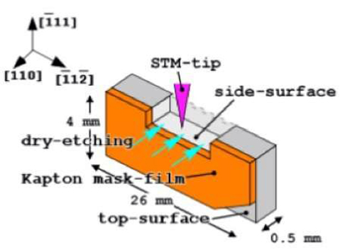
A schematics of a Si(110) sample with a Kapton film mask: dry etching from the (110) top-surface and STM-tip approaching to the (-111) side-surface. Image: Osaka University

A research collaboration between Osaka University and the Nara Institute of Science and Technology for the first time used scanning tunneling microscopy (STM) to create images of atomically flat side-surfaces of 3-D silicon crystals. This work helps semiconductor manufacturers continue to innovate while producing smaller, faster, and more energy-efficient computer chips for computers and smartphones.

Our computers and smartphones each are loaded with millions of tiny transistors. The processing speed of these devices has increased dramatically over time as the number of transistors that can fit on a single computer chip continues to increase. Based on Moore’s Law, the number of transistors per chip will double about every 2 years, and in this area it seems to be holding up. To keep up this pace of rapid innovation, computer manufacturers are continually on the lookout for new methods to make each transistor ever smaller.

Current microprocessors are made by adding patterns of circuits to flat silicon wafers. A novel way to cram more transistors in the same space is to fabricate 3-D-structures. Fin-type field effect transistors (FETs) are named as such because they have fin-like silicon structures that extend into the air, off the surface of the chip. However, this new method requires a silicon crystal with a perfectly flat top and side-surfaces, instead of just the top surface, as with current devices. Designing the next generation of chips will require new knowledge of the atomic structures of the side-surfaces.

Now, researchers at Osaka University and the Nara Institute of Science and Technology report that they have used STM to image the side-surface of a silicon crystal for the first time. STM is a powerful technique that allows the locations of the individual silicon atoms to be seen. By passing a sharp tip very close to the sample, electrons can jump across the gap and create an electrical current. The microscope monitored this current, and determined the location of the atoms in the sample.

“Our study is a big first step toward the atomically resolved evaluation of transistors designed to have 3-D-shapes,” study coauthor Azusa Hattori says.

To make the side-surfaces as smooth as possible, the researchers first treated the crystals with a process called reactive ion etching. Coauthor Hidekazu Tanaka says, “Our ability to directly look at the side-surfaces using STM proves that we can make artificial 3-D structures with near-perfect atomic surface ordering.”

Source: Osaka University

Related Articles Read More >

‘Self-driving’ lab speeds up research, synthesis of energy materials
Record-breaking, ultrafast devices step to protecting the grid from EMPs
Surprising semiconductor properties revealed with innovative new method
Thermo Scientific Centrios HX offers precise circuit edit solution for fast prototyping
2021 R&D Global Funding Forecast

Need R&D World news in a minute?

We Deliver!
R&D World Enewsletters get you caught up on all the mission critical news you need in research and development. Sign up today.
Enews Signup

R&D World Digital Issues

February 2020 issue

Browse the most current issue of R&D World and back issues in an easy to use high quality format. Clip, share and download with the leading R& magazine today.

Research & Development World
  • Subscribe to R&D World Magazine
  • Enews Sign Up
  • Contact Us
  • About Us
  • Drug Discovery & Development
  • Pharmaceutical Processing
  • 2022 Global Funding Forecast

Copyright © 2022 WTWH Media LLC. All Rights Reserved. The material on this site may not be reproduced, distributed, transmitted, cached or otherwise used, except with the prior written permission of WTWH Media
Privacy Policy | Advertising | About Us

Search R&D World

  • Home Page
  • Topics
    • Aerospace
    • Archeology
    • Automotive
    • Biotech
    • Chemistry
    • COVID-19
    • Environment
    • Energy
    • Life Science
    • Material Science
    • R&D Market Pulse
    • R&D Management
    • Physics
  • Technology
    • 3D Printing
    • A.I./Robotics
    • Battery Technology
    • Controlled Environments
      • Cleanrooms
      • Graphene
      • Lasers
      • Regulations/Standards
      • Sensors
    • Imaging
    • Nanotechnology
    • Scientific Computing
      • Big Data
      • HPC/Supercomputing
      • Informatics
      • Security
      • Software
    • Semiconductors
  • 2021 R&D 100 Award Winners
    • R&D 100 Awards
    • 2020 Winners
    • Winner Archive
  • Resources
    • Digital Issues
    • Podcasts
    • Subscribe
  • Global Funding Forecast
  • Webinars