 Researchers have developed a new approach for better integrating medical devices with biological systems. The researchers, led by Bozhi Tian, assistant professor in chemistry at the University of Chicago, have developed the first skeleton-like silicon spicules ever prepared via chemical processes.
“Using bone formation as a guide, the Tian group has developed a synthetic material from silicon that shows potential for improving interaction between soft tissue and hard materials,” says Joe Akkara, a program director in the National Science Foundation materials research division, which funded this research. “This is the power of basic scientific research. The Tian group has created a material that preliminarily seems to enhance soft tissue function.”
In a Science paper published on June 26, Tian and his co-authors from UChicago and Northwestern University described their new method for the syntheses and fabrication of mesocopic three-dimensional semiconductors — intermediate between the nanometer and macroscopic scales.
“This opens up a new opportunity for building electronics for enhanced sensing and stimulation at bio-interfaces,” says lead author Zhiqiang Luo, a postdoctoral scholar in Tian’s laboratory.
The team achieved three advances in the development of semiconductor and biological materials. One advance was the demonstration, by strictly chemical means, of three-dimensional lithography. Existing lithographic techniques create features over flat surfaces. The laboratory system mimics the natural reaction-diffusion process that leads to symmetry-breaking forms in nature: the grooved and notched form of a bee stinger, for example.
Tian’s team developed a pressure modulation synthesis, to promote the growth of silicon nanowires and to induce gold-based patterns in the silicon. Gold acts as silicon’s growth catalyst. By repeatedly increasing and decreasing the pressure on their samples, the researchers were able to control the gold’s precipitation and diffusion along the silicon’s faceted surfaces.
 “The idea of utilizing deposition-diffusion cycles can be applied to synthesizing more complex 3D semiconductors,” says co-lead author Yuanwen Jiang, a Seymour Goodman Fellow in chemistry at UChicago.
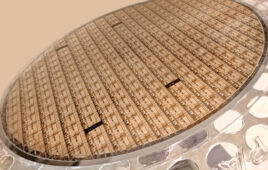
The semiconductor industry uses wet chemical etching with an etch resist to create planar patterns on silicon wafers. Portions of the wafer masked with thin film physically block the etching from being carried out, except on the open surface areas.
In another advance, Tian and his associates developed a novel chemical method that instead depends upon the uncanny ability of gold atoms to trap silicon-carrying electrons to selectively prevent the etching.
Much to their surprise, the researchers found that even a sparse cover of gold atoms over the silicon matrix would prevent etching from occurring in their proximity. This method also applies to the three-dimensional lithography of many other semiconductor compounds.
“This is a fundamentally new mechanism for etch mask or etch resist,” Tian says. “The entire process is chemical.”
Further testing revealed the project’s third advance. The testing showed that the synthetic silicon spicules displayed stronger interactions with collagen fibers — a skin-like stand-in for biological tissue — than did currently available silicon structures. Tian and his associates inserted the synthetic spicules and the other silicon structures into the collagen fibers, then pulled them out. An atomic force microscope measured the force required to accomplish each action.
“One of the major hurdles in the area of bioelectronics or implants is that the interface between the electronic device and the tissue or organ is not robust,” Tian says.
The spicules show promise for clearing this hurdle. They penetrated easily into the collagen, then became deeply rooted, much like a bee stinger in human skin.
Release Date: July 9, 2015
Source: University of Chicago


