UC Berkeley engineers have built a bright-light emitting device that is millimeters wide and fully transparent when turned off. The light emitting material in this device is a monolayer semiconductor, which is just three atoms thick.
The device opens the door to invisible displays on walls and windows – displays that would be bright when turned on but see-through when turned off — or in futuristic applications such as light-emitting tattoos, according to the researchers.
“The materials are so thin and flexible that the device can be made transparent and can conform to curved surfaces,” said Der-Hsien Lien, a postdoctoral fellow at UC Berkeley and a co-first author along with Matin Amani and Sujay Desai, both doctoral students in the Department of Electrical Engineering and Computer Sciences at Berkeley.
Their study was published March 26 in the journal Nature Communications. The work was funded by the National Science Foundation and the Department of Energy.
The device was developed in the laboratory of Ali Javey, professor of Electrical Engineering and Computer Sciences at Berkeley. In 2015, Javey’s lab published research in the journal Science showing that monolayer semiconductors are capable of emitting bright light, but stopped short of building a light-emitting device. The new work in Nature Communications overcame fundamental barriers in utilizing LED technology on monolayer semiconductors, allowing for such devices to be scaled from sizes smaller than the width of a human hair up to several millimeters. That means that researchers can keep the thickness small, but make the lateral dimensions (width and length) large, so that the light intensity can be high.
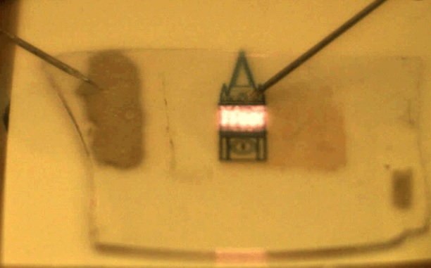
Probes inject positive and negative charges in the light emitting device, which is transparent under the campanile outline, producing bright light. Image: Taken from video by Javey lab
Commercial LEDs consist of a semiconductor material that is electrically injected with positive and negative charges, which produce light when they meet. Typically, two contact points are used in a semiconductor-based light emitting device; one for injecting negatively charged particles and one injecting positively charged particles. Making contacts that can efficiently inject these charges is a fundamental challenge for LEDs, and it is particularly challenging for monolayer semiconductors since there is so little material to work with.
The Berkeley research team engineered a way to circumvent this challenge by designing a new device that only requires one contact on the semiconductor. By laying the semiconductor monolayer on an insulator and placing electrodes on the monolayer and underneath the insulator, the researchers could apply an AC signal across the insulator. During the moment when the AC signal switches its polarity from positive to negative (and vice versa), both positive and negative charges are present at the same time in the semiconductor, creating light.
The researchers showed that this mechanism works in four different monolayer materials, all of which emit different colors of light.
This device is a proof-of-concept, and much research still remains, primarily to improve efficiency. Measuring this device’s efficiency is not straightforward, but the researchers think it’s about 1 percent efficient. Commercial LEDs have efficiencies of around 25 to 30 percent.
The concept may be applicable to other devices and other kinds of materials, the device could one day have applications in a number of fields where having invisible displays are warranted. That could be an atomically thin display that’s imprinted on a wall or even on human skin.
“A lot of work remains to be done and a number of challenges need to be overcome to further advance the technology for practical applications,” Javey says. “However, this is one step forward by presenting a device architecture for easy injection of both charges into monolayer semiconductors.”
Source: UC Berkeley


