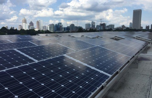
Rows of photovoltaic panels are shown atop a building on the Georgia Institute of Technology campus in Atlanta. Credit: John Toon, Georgia Tech
A team of semiconductor researchers based in France has used a boron nitride separation layer to grow indium gallium nitride (InGaN) solar cells that were then lifted off their original sapphire substrate and placed onto a glass substrate.
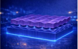
By combining the InGaN cells with photovoltaic (PV) cells made from materials such as silicon or gallium arsenide, the new lift-off technique could facilitate fabrication of higher efficiency hybrid PV devices able to capture a broader spectrum of light. Such hybrid structures could theoretically boost solar cell efficiency as high as 30 percent for an InGaN/Si tandem device.
The technique is the third major application for the hexagonal boron nitride lift-off technique, which was developed by a team of researchers from the Georgia Institute of Technology, the French National Center for Scientific Research (CNRS), and Institut Lafayette in Metz, France. Earlier applications targeted sensors and light-emitting diodes (LEDs).
“By putting these structures together with photovoltaic cells made of silicon or a III-V material, we can cover the visible spectrum with the silicon and utilize the blue and UV light with indium gallium nitride to gather light more efficiently,” said Abdallah Ougazzaden, director of Georgia Tech Lorraine in Metz, France and a professor in Georgia Tech’s School of Electrical and Computer Engineering (ECE). “The boron nitride layer doesn’t impact the quality of the indium gallium nitride grown on it, and we were able to lift off the InGaN solar cells without cracking them.”
The research was published August 15 in the journal ACS Photonics. It was supported by the French National Research Agency under the GANEX Laboratory of Excellence project and the French PIA project “Lorraine Université d’Excellence.”
The technique could lead to production of solar cells with improved efficiency and lower cost for a broad range of terrestrial and space applications. “This demonstration of transferred InGaN-based solar cells on foreign substrates while increasing performance represents a major advance toward lightweight, low cost, and high efficiency photovoltaic applications,” the researchers wrote in their paper.
“Using this technique, we can process InGaN solar cells and put a dielectric layer on the bottom that will collect only the short wavelengths,” Ougazzaden explained. “The longer wavelengths can pass through it into the bottom cell. By using this approach we can optimize each surface separately.”
The researchers began the process by growing monolayers of boron nitride on two-inch sapphire wafers using an MOVPE process at approximately 1,300 degrees Celsius. The boron nitride surface coating is only a few nanometers thick, and produces crystalline structures that have strong planar surface connections, but weak vertical connections.
The InGaN attaches to the boron nitride with weak van der Waals forces, allowing the solar cells to be grown across the wafer and removed without damage. So far, the cells have been removed from the sapphire manually, but Ougazzaden believes the transfer process could be automated to drive down the cost of the hybrid cells. “We can certainly do this on a large scale,” he said.
The InGaN structures are then placed onto the glass substrate with a backside reflector and enhanced performance is obtained. Beyond demonstrating placement atop an existing PV structure, the researchers hope to increase the amount of indium in their lift-off devices to boost light absorption and increase the number of quantum wells from five to 40 or 50.
“We have now demonstrated all the building blocks, but now we need to grow a real structure with more quantum wells,” Ougazzaden said. “We are just at the beginning of this new technology application, but it is very exciting.”
In addition to Ougazzaden, the research team includes Georgia Tech Ph.D. students Taha Ayari, Matthew Jordan, Xin Li and Saiful Alam; Chris Bishop and Simon Gautier from Institut Lafayette; Suresh Sundaram, a researcher at Georgia Tech Lorraine; Walid El Huni and Yacine Halfaya from CNRS; Paul Voss, an associate professor in the Georgia Tech School of ECE; and Jean Paul Salvestrini, a professor at Georgia Tech Lorraine and adjunct professor in the Georgia Tech School of ECE.