Research & Development World

  • R&D World Home
  • Topics
    • Aerospace
    • Automotive
    • Biotech
    • Careers
    • Chemistry
    • Environment
    • Energy
    • Life Science
    • Material Science
    • R&D Management
    • Physics
  • Technology
    • 3D Printing
    • A.I./Robotics
    • Software
    • Battery Technology
    • Controlled Environments
      • Cleanrooms
      • Graphene
      • Lasers
      • Regulations/Standards
      • Sensors
    • Imaging
    • Nanotechnology
    • Scientific Computing
      • Big Data
      • HPC/Supercomputing
      • Informatics
      • Security
    • Semiconductors
  • R&D Market Pulse
  • R&D 100
    • Call for Nominations: The 2025 R&D 100 Awards
    • R&D 100 Awards Event
    • R&D 100 Submissions
    • Winner Archive
    • Explore the 2024 R&D 100 award winners and finalists
  • Resources
    • Research Reports
    • Digital Issues
    • R&D Index
    • Subscribe
    • Video
    • Webinars
  • Global Funding Forecast
  • Top Labs
  • Advertise
  • SUBSCRIBE

Chemically Tailored Graphene Used in Semiconductor Applications

By University of Vienna | May 8, 2017

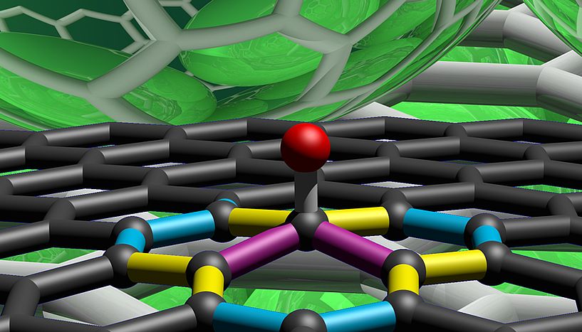
Section of a graphene network with chemically bound hydrogen atom: the spectral vibrational signature of the single carbon-carbon bonds adjacent to the bound hydrogen atom is highlighted in different colors Image: Copyright Frank Hauke, FAU

Graphene is considered to be one of the most promising new materials. However, the systematic insertion of chemically bound atoms and molecules to control its properties is still a major challenge. Now, for the first time, scientists of the Friedrich-Alexander-Universität Erlangen-Nürnberg, the University of Vienna, the Freie Universität Berlin, and the University Yachay Tech in Ecuador succeeded in precisely verifying the spectral fingerprint of such compounds in both theory and experiment. Their results are published in the scientific journal Nature Communications.

Two-dimensional graphene consists of single layers of carbon atoms and exhibits intriguing properties. The transparent material conducts electricity and heat extremely well. It is at the same time flexible and solid. Additionally, the electrical conductivity can be continuously varied between a metal and a semiconductor by, e.g., inserting chemically bound atoms and molecules into the graphene structure — the so-called functional groups. These unique properties offer a wide range of future applications as e.g. for new developments in optoelectronics or ultrafast components in the semiconductor industry. However, a successful use of graphene in the semiconductor industry can only be achieved if properties such as the conductivity, the size and the defects of the graphene structure induced by the functional groups can already be modulated during the synthesis of graphene.

In an international collaboration scientists led by Andreas Hirsch from the Friedrich-Alexander-Universität Erlangen-Nürnberg in close cooperation with Thomas Pichler from the University of Vienna accomplished a crucial breakthrough: using the latter’s newly developed experimental set-up they were able to identify, for the first time, vibrational spectra as the specific fingerprints of step-by-step chemically modified graphene by means of light scattering. This spectral signature, which was also theoretically attested, allows to determine the type and the number of functional groups in a fast and precise way. Among the reactions they examined, was the chemical binding of hydrogen to graphene. This was implemented by a controlled chemical reaction between water and particular compounds in which ions are inserted in graphite, a crystalline form of carbon.

“This method of the in-situ Raman spectroscopy is a highly effective technique which allows controlling the function of graphene in a fast, contact-free and extensive way already during the production of the material,” says J. Chacon from Yachay Tech, one of the two lead authors of the study. This enables the production of tailored graphene-based materials with controlled electronic transport properties and their utilization in semiconductor industry.

Source: University of Vienna

Related Articles Read More >

The emerging materials shaping next-generation semiconductor electronics
24 R&D trends that redefined 2024
Graphene-based flowmeter sensor measures nano-rate fluid flows, Part 3: The sensor
Graphene-based flowmeter sensor measures nano-rate fluid flows, Part 2: The graphene context
rd newsletter
EXPAND YOUR KNOWLEDGE AND STAY CONNECTED
Get the latest info on technologies, trends, and strategies in Research & Development.
RD 25 Power Index

R&D World Digital Issues

Fall 2024 issue

Browse the most current issue of R&D World and back issues in an easy to use high quality format. Clip, share and download with the leading R&D magazine today.

Research & Development World
  • Subscribe to R&D World Magazine
  • Enews Sign Up
  • Contact Us
  • About Us
  • Drug Discovery & Development
  • Pharmaceutical Processing
  • Global Funding Forecast

Copyright © 2025 WTWH Media LLC. All Rights Reserved. The material on this site may not be reproduced, distributed, transmitted, cached or otherwise used, except with the prior written permission of WTWH Media
Privacy Policy | Advertising | About Us

Search R&D World

  • R&D World Home
  • Topics
    • Aerospace
    • Automotive
    • Biotech
    • Careers
    • Chemistry
    • Environment
    • Energy
    • Life Science
    • Material Science
    • R&D Management
    • Physics
  • Technology
    • 3D Printing
    • A.I./Robotics
    • Software
    • Battery Technology
    • Controlled Environments
      • Cleanrooms
      • Graphene
      • Lasers
      • Regulations/Standards
      • Sensors
    • Imaging
    • Nanotechnology
    • Scientific Computing
      • Big Data
      • HPC/Supercomputing
      • Informatics
      • Security
    • Semiconductors
  • R&D Market Pulse
  • R&D 100
    • Call for Nominations: The 2025 R&D 100 Awards
    • R&D 100 Awards Event
    • R&D 100 Submissions
    • Winner Archive
    • Explore the 2024 R&D 100 award winners and finalists
  • Resources
    • Research Reports
    • Digital Issues
    • R&D Index
    • Subscribe
    • Video
    • Webinars
  • Global Funding Forecast
  • Top Labs
  • Advertise
  • SUBSCRIBE