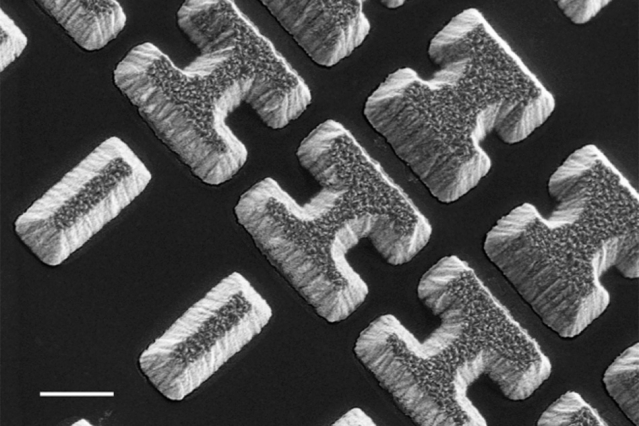
Scanning Electron Microscope image shows a few of the carefully designed shaped of the chalcogenide glass deposited on a clear substrate. The shapes, which the researchers call “meta-atoms,” determine how mid-infrared light is bent when passing through the material. Image: Courtesy of the researchers
A new way of taking images in the mid-infrared part of the spectrum, developed by researchers at MIT and elsewhere, could enable a wide variety of applications, including thermal imaging, biomedical sensing, and free-space communication.
The mid-infrared (mid-IR) band of electromagnetic radiation is a particularly useful part of the spectrum; it can provide imaging in the dark, trace heat signatures, and provide sensitive detection of many biomolecular and chemical signals. But optical systems for this band of frequencies have been hard to make, and devices using them are highly specialized and expensive. Now, the researchers say they have found a highly efficient and mass-manufacturable approach to controlling and detecting these waves.
The findings are reported in the journal Nature Communications, in a paper by MIT researchers Tian Gu and Juejun Hu, University of Massachusetts at Lowell researcher Hualiang Zhang, and 13 others at MIT, the University of Electronic Science and Technology of China, and the East China Normal University.
The new approach uses a flat, artificial material composed of nanostructured optical elements, instead of the usual thick, curved-glass lenses used in conventional optics. These elements provide on-demand electromagnetic responses and are made using techniques similar to those used for computer chips. “This kind of metasurface can be made using standard microfabrication techniques,” Gu says. “The manufacturing is scalable.”
He adds that “there have been remarkable demonstrations of metasurface optics in visible light and near-infrared, but in the mid-infrared it’s moving slowly.” As they began this research, he says, the question was, since they could make these devices extremely thin, “Could we also make them efficient and low-cost?” That’s what the team members say they have now achieved.
The new device uses an array of precisely shaped thin-film optical elements called “meta-atoms” made of chalcogenide alloy, which has a high refractive index that can form high-performance, ultrathin structures called meta-atoms. These meta-atoms, with shapes resembling block letters like I or H, are deposited and patterned on an IR-transparent substrate of fluoride. The tiny shapes have thicknesses that are a fraction of the wavelengths of the light being observed, and collectively they can perform like a lens. They provide nearly arbitrary wavefront manipulation that’s not possible with natural materials at larger scales, but they have a tiny fraction of the thickness, and thus only a tiny amount of material is needed. “It’s fundamentally different from conventional optics,” he says.
The process “allows us to use very simple fabrication techniques,” Gu explains, by thermally evaporating the material onto the substrate. They have demonstrated the technique on 6-inch wafers with high throughput, a standard in microfabrication, and “we’re looking at even larger-scale manufacturing.”
The devices transmit 80 percent of the mid-IR light with optical efficiencies up to 75 percent, representing significant improvement over existing mid-IR metaoptics, Gu says. They can also be made far lighter and thinner than conventional IR optics. Using the same method, by varying the pattern of the array the researchers can arbitrarily produce different types of optical devices, including a simple beam deflector, a cylindrical or spherical lens, and complex aspheric lenses. The lenses have been demonstated to focus mid-IR light with the maximum theoretically possible sharpness, known as the diffraction limit.
These techniques allow the creation of metaoptical devices, which can manipulate light in more complex ways than what can be achieved using conventional bulk transparent materials, Gu says. The devices can also control polarization and other properties.
Mid-IR light is important in many fields. It contains the characteristic spectral bands of most types of molecules, and penetrates the atmosphere effectively, so it is key to detecting a wide range of substances such as in environmental monitoring, as well as for military and industrial applications, the researchers say. Since most ordinary optical materials used in the visible or near-infrared bands are totally opaque to these wavelengths, mid-IR sensors have been complex and expensive to make. So the new approach could open up entirely new potential applications, including in consumer sensing or imaging products, Gu says.
The research was funded by the Defense Advanced Research Projects Agency (DARPA), under the Extreme Optics and Imaging Program, and the National Natural Science Foundation of China.
Source: MIT