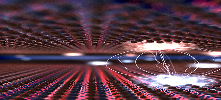
When atomically thin layers of two materials are stacked and twisted, a ‘heterostructure’ material emerges. A new connection is formed, almost instantaneously, with special energy states – known as interlayer excitons – that exist in both layers and determine the properties of the new material. Illustration: Brad Baxley
Through magic twist angles and unique energy states, it is possible to design tailor-made, atomically thin materials that could be invaluable for future electronics. Now, researchers at Chalmers University of Technology, Sweden, and Regensburg University in Germany have shed light on the ultrafast dynamics in these novel materials. The results were recently published in the prestigious journal Nature Materials.
Imagine you are building an energy-efficient and super-thin solar cell. You have one material that conducts current and another that absorbs light. You must therefore use both materials to achieve the desired properties, and the result may not be as thin as you hoped.
Now imagine instead that you have atomically thin layers of each material, that you place on top of each other. You twist one layer towards the other a certain amount, and suddenly a new connection is formed, with special energy states—known as interlayer excitons—that exist in both layers. You now have your desired material at an atomically thin level.
Ermin Malic, researcher at Chalmers University of Technology, in collaboration with German research colleagues around Rupert Huber at Regensburg University, has now succeeded in showing how fast these states are formed and how they can be tuned through twisting angles. Stacking and twisting atomically thin materials like Lego bricks, into new materials known as “heterostructures,” is an area of research that is still at its beginning.
“These heterostructures have tremendous potential, as we can design tailor-made materials. The technology could be used in solar cells, flexible electronics, and even possibly in quantum computers in the future,” says Malic, Professor at the Department of Physics at Chalmers.
Malic and his doctoral students Simon Ovesen and Samuel Brem recently collaborated with researchers at Regensburg University. The Swedish group has been responsible for the theoretical part of the project, while the German researchers conducted the experiments.
For the first time, with the help of unique methods, they succeeded in revealing the secrets behind the ultrafast formation and dynamics of interlayer excitons in heterostructure materials. They used two different lasers to follow the sequence of events. By twisting atomically thin materials towards each other, they have demonstrated that it is possible to control how quickly the exciton dynamics occurs.
“This emerging field of research is equally fascinating and interesting for academia as it is for industry,” says Malic.
He leads the Chalmers Graphene Centre, which gathers research, education and innovation around graphene, other atomically thin materials and heterostructures under one common umbrella.
These kinds of promising materials are known as two-dimensional (2D) materials, as they only consist of an atomically thin layer. Due to their remarkable properties, they are considered to have great potential in various fields of technology. Graphene, consisting of a single layer of carbon atoms, is the best-known example. It is starting to be applied in industry, for example in super-fast and highly sensitive detectors, flexible electronic devices and multifunctional materials in automotive, aerospace and packaging industries.
But graphene is just one of many 2D materials that could be of great benefit to our society. There is currently a lot of discussion about heterostructures consisting of graphene combined with other 2D materials. In just a short time, research on heterostructures has made great advances, and the journal Nature has recently published several breakthrough articles in this field of research.
At Chalmers, several research groups are working at the forefront of graphene. The Graphene Centre is now investing in new infrastructure in order to be able to broaden the research area to include other 2D materials and heterostructures as well.
“We want to establish a strong and dynamic hub for 2D materials here at Chalmers, so that we can build bridges to industry and ensure that our knowledge will benefit society,” says Malic.