Research & Development World

  • R&D World Home
  • Topics
    • Aerospace
    • Automotive
    • Biotech
    • Careers
    • Chemistry
    • Environment
    • Energy
    • Life Science
    • Material Science
    • R&D Management
    • Physics
  • Technology
    • 3D Printing
    • A.I./Robotics
    • Software
    • Battery Technology
    • Controlled Environments
      • Cleanrooms
      • Graphene
      • Lasers
      • Regulations/Standards
      • Sensors
    • Imaging
    • Nanotechnology
    • Scientific Computing
      • Big Data
      • HPC/Supercomputing
      • Informatics
      • Security
    • Semiconductors
  • R&D Market Pulse
  • R&D 100
    • Call for Nominations: The 2025 R&D 100 Awards
    • R&D 100 Awards Event
    • R&D 100 Submissions
    • Winner Archive
    • Explore the 2024 R&D 100 award winners and finalists
  • Resources
    • Research Reports
    • Digital Issues
    • R&D Index
    • Subscribe
    • Video
    • Webinars
  • Global Funding Forecast
  • Top Labs
  • Advertise
  • SUBSCRIBE

Decal Stickers Function as Semiconductors

By LMU Munich | May 8, 2017

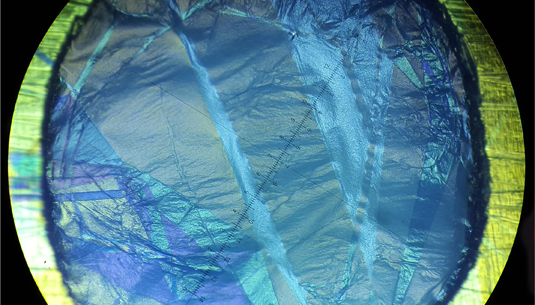
A 50nm pentacene film spanned across a 2 mm hole. Image: Simon Noever, LMU

Today’s computer processors are composed of billions of transistors. These electronic components normally consist of semiconductor material, insulator, substrate, and electrode. A dream of many scientists is to have each of these elements available as transferable sheets, which would allow them to design new electronic devices simply by stacking.

This has now become a reality for the organic semiconductor material pentacene: Dr. Bert Nickel, a physicist at LMU Munich, and Professor Andrey Turchanin (Friedrich Schiller University Jena), together with their teams, have, for the first time, managed to create mechanically stable pentacene nanosheets.

The researchers describe their method in the journal Advanced Materials. They first cover a small silicon wafer with a thin layer of a water-soluble organic film and deposit pentacene molecules upon it until a layer roughly 50 nanometers thick has formed. The next step is crucial: by irradiation with low-energy electrons, the topmost three to four levels of pentacene molecular layers are crosslinked, forming a “skin” that is only about five nanometers thick. This crosslinked layer stabilizes the entire pentacene film so well that it can be removed as a sheet from a silicon wafer in water and transferred to another surface using ordinary tweezers.

Apart from the ability to transfer them, the new semiconductor nanosheets have other advantages. The new method does not require any potentially interfering solvents, for example. In addition, after deposition, the nanosheet sticks firmly to the electrical contacts by van der Waals forces, resulting in a low contact resistance of the final electronic devices. Last but not least, organic semiconductor nanosheets can now be deposited onto significantly more technologically relevant substrates than hitherto.

Of particular interest is the extremely high mechanical stability of the newly developed pentacene nanosheets, which enables them to be applied as free-standing nanomembranes to perforated substrates with dimensions of tens of micrometers. That is equivalent to spanning a 25-meter pool with plastic wrap.

“These virtually freely suspended semiconductors have great potential,” explains Nickel. “They can be accessed from two sides and could be connected through an electrolyte, which would make them ideal as biosensors, for example.”

“Another promising application is their implementation in flexible electronics for manufacturing of devices for vital data acquisition or production of displays and solar cells,” Turchanin says.

Source: LMU Munich

Related Articles Read More >

TSMC’s N3P hits mass production, with N3X customer sampling slated for Q3–Q4 2025a
7 major R&D developments this week: Tariff uncertainty persists, Pfizer sells campus, Scania acquires Northvolt unit
While Trump tariffs spare phones/PCs, R&D could faces GPU cost pressures
Why IBM predicts quantum advantage within two years
rd newsletter
EXPAND YOUR KNOWLEDGE AND STAY CONNECTED
Get the latest info on technologies, trends, and strategies in Research & Development.
RD 25 Power Index

R&D World Digital Issues

Fall 2024 issue

Browse the most current issue of R&D World and back issues in an easy to use high quality format. Clip, share and download with the leading R&D magazine today.

Research & Development World
  • Subscribe to R&D World Magazine
  • Enews Sign Up
  • Contact Us
  • About Us
  • Drug Discovery & Development
  • Pharmaceutical Processing
  • Global Funding Forecast

Copyright © 2025 WTWH Media LLC. All Rights Reserved. The material on this site may not be reproduced, distributed, transmitted, cached or otherwise used, except with the prior written permission of WTWH Media
Privacy Policy | Advertising | About Us

Search R&D World

  • R&D World Home
  • Topics
    • Aerospace
    • Automotive
    • Biotech
    • Careers
    • Chemistry
    • Environment
    • Energy
    • Life Science
    • Material Science
    • R&D Management
    • Physics
  • Technology
    • 3D Printing
    • A.I./Robotics
    • Software
    • Battery Technology
    • Controlled Environments
      • Cleanrooms
      • Graphene
      • Lasers
      • Regulations/Standards
      • Sensors
    • Imaging
    • Nanotechnology
    • Scientific Computing
      • Big Data
      • HPC/Supercomputing
      • Informatics
      • Security
    • Semiconductors
  • R&D Market Pulse
  • R&D 100
    • Call for Nominations: The 2025 R&D 100 Awards
    • R&D 100 Awards Event
    • R&D 100 Submissions
    • Winner Archive
    • Explore the 2024 R&D 100 award winners and finalists
  • Resources
    • Research Reports
    • Digital Issues
    • R&D Index
    • Subscribe
    • Video
    • Webinars
  • Global Funding Forecast
  • Top Labs
  • Advertise
  • SUBSCRIBE