Even though nanographene is insoluble in water and organic solvents, Kumamoto University (KU) and Tokyo Institute of Technology (Tokyo Tech) researchers have found a way to dissolve it in water. Using “molecular containers” that encapsulate water-insoluble molecules, the researchers developed a formation procedure for a nanographene adlayer, a layer that chemically interacts with the underlying substance, by just mixing the molecular containers and nanographene together in water.
The method is expected to be useful for the fabrication and analysis of next-generation functional nanomaterials.
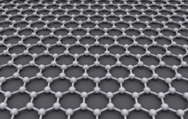
Graphene is a single layer of carbon atoms arranged in sheet form. It is lighter than metal with superior electrical characteristics, and has attracted attention as a next-generation material for electronics. Structurally defined nano-sized graphene, i.e. nanographene, has different physical properties from graphene.
Although nanographene is an attractive material for organic semiconductors and molecular devices, its molecular group is insoluble in many solvents, and its fundamental physical properties are not sufficiently understood.
Micelles can be used to dissolve water-insoluble substances in water. Soap is a familiar example of a micelle. When soap micelles mix with water, bubbles that are hydrophobic on the inside and hydrophilic on the outside begin to form. These bubbles trap oil-based dirt and make it easier to wash away with water.
Dr. Michito Yoshizawa of Tokyo Tech used this property of micelles to develop amphipathic (molecules that have both hydrophobic and hydrophilic properties) micelle capsules. Expanding upon Yoshizawa’s work, researchers at KU developed a micelle capsule for insoluble nanographene compound groups.
The KU researchers utilized micelle capsules composed of specific chemical structures (anthracene) as molecular containers and skillfully made use of molecule interactions to efficiently intake nanographene molecules into the capsules.
The micelle capsules act like presents from Santa Claus, the highly hydrophobic nanographene molecules (the toy) inside the capsule (the box/wrapping paper) are transported to the surface of the gold (Au) substrate underwater (the Christmas tree).
The micelle capsules then undergo a change of molecular state (equilibrium) in the acidic aqueous solution. The nanographene that was inside the micelle is adsorbed and organized on the Au substrate, since without its “protective wrapping” it is not dissolved in water.
Using an Electrochemical Scanning Tunneling Microscope (EC-STM), which resolves material surfaces at the atomic level, the researchers successfully observed three types of nanographene molecules (ovalene, circobiphenyl, and dicoronylene) in molecular-scale resolution for the first time in the world. The images showed that the molecules adsorbed on the Au substrate were regularly aligned and formed a highly ordered 2D molecular adlayer.
This method of molecular adlayer fabrication uses molecules with solubility limitations but it can also be used for other types of molecules as well. Moreover, it should attract attention as an eco-friendly technology since it does not require the use of harmful organic solvents. The research team expects it to open new doors in nanographene science research.
“A couple of years ago, KU faced significant challenges due to the 2016 Kumamoto earthquakes. While we were recovering from this disaster, Tokyo Tech accepted senior undergraduate students from our laboratory as special auditors. This collaborative research project started from that point. The results of this work are a direct result of Tokyo Tech’s rapid response and kind cooperation during the difficult situation we faced here in Kumamoto. We really appreciate their generous assistance,” says project leader Associate Professor Soichiro Yoshimoto of Kumamoto University.
“The method we developed can also be applied to a group of molecules with a larger chemical structure. We expect to see this work lead to the development of molecular wires, new battery materials, thin film crystal growth from precise molecular designs, and the further elucidation of fundamental physical properties.”
This research result was posted in Angewandte Chemie International Edition on Oct. 23, 2018.
Source: Kumamoto University


