Research & Development World

  • R&D World Home
  • Topics
    • Aerospace
    • Automotive
    • Biotech
    • Careers
    • Chemistry
    • Environment
    • Energy
    • Life Science
    • Material Science
    • R&D Management
    • Physics
  • Technology
    • 3D Printing
    • A.I./Robotics
    • Software
    • Battery Technology
    • Controlled Environments
      • Cleanrooms
      • Graphene
      • Lasers
      • Regulations/Standards
      • Sensors
    • Imaging
    • Nanotechnology
    • Scientific Computing
      • Big Data
      • HPC/Supercomputing
      • Informatics
      • Security
    • Semiconductors
  • R&D Market Pulse
  • R&D 100
    • Call for Nominations: The 2025 R&D 100 Awards
    • R&D 100 Awards Event
    • R&D 100 Submissions
    • Winner Archive
    • Explore the 2024 R&D 100 award winners and finalists
  • Resources
    • Research Reports
    • Digital Issues
    • R&D Index
    • Subscribe
    • Video
    • Webinars
  • Global Funding Forecast
  • Top Labs
  • Advertise
  • SUBSCRIBE

Elusive charge properties of plasmons quantified

By R&D Editors | July 19, 2011

SurfacePlasmon1

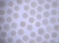
Imaging plasmonic charge separation.

Surface
plasmons, or the collective oscillations of electrical charge on the
surfaces of metals, are of considerable interest to scientists primarily
for their potential to control light on the nanoscale, far beyond the
limits of conventional optics. At such minute dimensions, however, the
precise properties of the individual plasmonic resonances are difficult
to determine.

Emiko
Kazuma, Nobuyuki Sakai and Tetsu Tatsuma from the Institute of
Industrial Science at the University of Tokyo in Japan have now
developed a technique for imaging the electrical charge separation sites
of individual plasmonic nanoparticles, which could lead to better
tuning of their plasmonic properties.    

The
electromagnetic fields of plasmonic nanostructures can take complex
forms and are strongly influenced by factors such as the wavelength of
light or the geometry of the metallic nanostructures. Tatsuma and his
colleagues overcame the difficulty in imaging these nanoscale fields by
developing an indirect approach. They grew plasmonic silver
nanostructures on titanium dioxide to construct a system in which
plasmon-induced electric charges in the silver transfer to the titanium
dioxide. In a humid atmosphere, the silver ions formed by this charge
transfer become dissolved in water adsorbed to the sample surface and
redeposit on the titanium dioxide surface as silver nanoparticles.

As
the number of dissolved silver ions depends directly on the number of
electronic charges, the distribution of these silver nanoparticles
around the plasmonic structure is an indicator of the original electric
field distribution. Imaging these nanoparticles, which can be easily
done using a microscope, then provides an indirect indicator of the
electric field distribution (see image).

This
method has important consequences for the development of plasmonic
devices, says Tatsuma. “Now we can improve the efficiency of the
plasmon-induced charge separation by designing structures where the
plasmonic fields are strong.” In particular, he adds, this could be used
to optimize fabrication processes. As plasmonic structures are
typically only a few nanometers in size, small structural deviations
have a significant effect on their plasmonic properties. This new
methodology could therefore prove to be an important diagnostic tool for
scientists in the development of enhanced plasmonic devices.

Nanoimaging of localized plasmon-induced charge separation

SOURCE:  Tokyo Institute of Technology

Related Articles Read More >

KIST carbon nanotube supercapacitor holds capacity after 100,000 cycles
A new wave of metalworking lets semiconductor crystals bend and stretch
LLNL deposits quantum dots on corrugated IR chips in a single step
KATRIN inauguration photo form 2018
Neutrinos pinned below 0.45 eV; KATRIN halves the particle’s mass ceiling
rd newsletter
EXPAND YOUR KNOWLEDGE AND STAY CONNECTED
Get the latest info on technologies, trends, and strategies in Research & Development.
RD 25 Power Index

R&D World Digital Issues

Fall 2024 issue

Browse the most current issue of R&D World and back issues in an easy to use high quality format. Clip, share and download with the leading R&D magazine today.

Research & Development World
  • Subscribe to R&D World Magazine
  • Enews Sign Up
  • Contact Us
  • About Us
  • Drug Discovery & Development
  • Pharmaceutical Processing
  • Global Funding Forecast

Copyright © 2025 WTWH Media LLC. All Rights Reserved. The material on this site may not be reproduced, distributed, transmitted, cached or otherwise used, except with the prior written permission of WTWH Media
Privacy Policy | Advertising | About Us

Search R&D World

  • R&D World Home
  • Topics
    • Aerospace
    • Automotive
    • Biotech
    • Careers
    • Chemistry
    • Environment
    • Energy
    • Life Science
    • Material Science
    • R&D Management
    • Physics
  • Technology
    • 3D Printing
    • A.I./Robotics
    • Software
    • Battery Technology
    • Controlled Environments
      • Cleanrooms
      • Graphene
      • Lasers
      • Regulations/Standards
      • Sensors
    • Imaging
    • Nanotechnology
    • Scientific Computing
      • Big Data
      • HPC/Supercomputing
      • Informatics
      • Security
    • Semiconductors
  • R&D Market Pulse
  • R&D 100
    • Call for Nominations: The 2025 R&D 100 Awards
    • R&D 100 Awards Event
    • R&D 100 Submissions
    • Winner Archive
    • Explore the 2024 R&D 100 award winners and finalists
  • Resources
    • Research Reports
    • Digital Issues
    • R&D Index
    • Subscribe
    • Video
    • Webinars
  • Global Funding Forecast
  • Top Labs
  • Advertise
  • SUBSCRIBE