The Sydney Nanoscience Hub, headquarters of the Australian Institute for Nanoscale Science and Technology (AINST), will officially launch on April 20.
The new $150 million facility is among the most sophisticated laboratories for advanced measurement and experimental device demonstration globally built for this purpose and joins just a handful of facilities at some of the most prominent universities around the world.

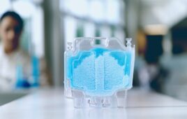
 Available for public use is a one-stop-shop prototyping facility and cleanroom (including core facilities in nanofabrication, nanometrology, and nanoscale imaging). These facilities will be complemented by an advanced electron microscope in one of the most electromagnetically and mechanically stable laboratory environments in the world.
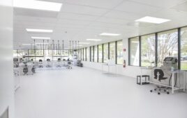
The facility — measuring approximately 11,600 square meters in size — is a world-first, offering combinations of laboratories with unprecedented technical performance for nanoscale research, meshed with teaching facilities that bring students into the heart of the action.
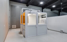
The research laboratories span a variety of specifications, but these “precision metrology” laboratories have combinations of technical performance that are unmatched in comparable facilities globally. These include extremely tight electromagnetic interference specifications (<10nT pp fluctuations); vibration (better than VCG criterion — the tightest spec developed — a particular metric for floor vibration over a frequency band); air temperature stability (temp stable to within +/- 0.1 C); air pressure (fluctuations <~5-7 Pa); and humidity (stable +/-5 percent).
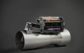
The Institute is also about to commence the procurement process for a new aberration corrected transmission electron microscope. This microscope will allow researchers to “see” and measure atoms and the forces that bind them together.
 The Sydney Nanoscience Hub was completed in 2015. The project team consists of Professor Thomas Maschmeyer, AINST Director; Professor Simon Ringer, Director, Sydney Nanoscience Hub and Research and Prototype Foundry; and Professor Zdenka Kuncic, Director, Community and Research.
Professor Simon Ringer is the Director of the Sydney Nanoscience Hub. [email protected]
This article appeared in the March/April 2016 issue of Controlled Environments.