Research & Development World

  • R&D World Home
  • Topics
    • Aerospace
    • Automotive
    • Biotech
    • Careers
    • Chemistry
    • Environment
    • Energy
    • Life Science
    • Material Science
    • R&D Management
    • Physics
  • Technology
    • 3D Printing
    • A.I./Robotics
    • Software
    • Battery Technology
    • Controlled Environments
      • Cleanrooms
      • Graphene
      • Lasers
      • Regulations/Standards
      • Sensors
    • Imaging
    • Nanotechnology
    • Scientific Computing
      • Big Data
      • HPC/Supercomputing
      • Informatics
      • Security
    • Semiconductors
  • R&D Market Pulse
  • R&D 100
    • Call for Nominations: The 2025 R&D 100 Awards
    • R&D 100 Awards Event
    • R&D 100 Submissions
    • Winner Archive
    • Explore the 2024 R&D 100 award winners and finalists
  • Resources
    • Research Reports
    • Digital Issues
    • R&D Index
    • Subscribe
    • Video
    • Webinars
  • Global Funding Forecast
  • Top Labs
  • Advertise
  • SUBSCRIBE

Graphene Layers Caught “Kissing”

By University of Leiden | March 26, 2018

University of Leiden physicists and chemists have managed to bring two graphene layers so close together that an electric current spontaneously jumps across. In the future, this could enable scientists to study the edges of graphene and use them for sequencing DNA with a precision beyond existing technologies. The study has been published in Nano Letters.

How do you study an object that is so small it won’t even reflect light? In this case, physicists like to send a current through to measure its conductance, which gives away many properties. Still, if you have something extremely small, such as a molecule, this is easier said than done. You will need electrodes smaller than the molecule. Leiden research teams of physicist Jan van Ruitenbeek and chemist Grégory F. Schneider devised a way to dodge this problem. They tilted two one-atom-thick sheets of graphene such that they only meet in one point, where electrons jump across from one layer to the other.

Previous attempts with graphene electrodes failed because the layers are floppy by nature. The Leiden scientists deposited them on a silicon substrate, making them rigid all the way to the edge. They brought both layers close enough together so that tunneling occurs — a quantum mechanical phenomenon where electrons spontaneously jump to a neighboring material, even though there is no direct contact. Any small object in between will enhance the tunneling. The number of electrons tunneling through will tell researchers about some of its properties.

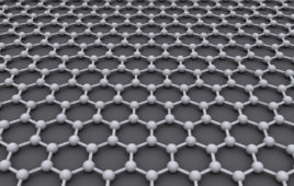
Image: Amedeo Bellunato

One promising future application could be DNA sequencing. As a single DNA strand passes through the tight gap between the graphene layers, its nucleotide letters A, C, G, and T will alternately allow a different number of electrons to tunnel through. From this, scientists might be able to read out a DNA strand relatively quickly.

van Ruitenbeek says, “Companies are now developing another method where they run a DNA strand through a hole which also has water flowing through with electrically charged particles. From the strength of the current they know which base letter is partly blocking the hole. Our method is potentially much more accurate. Or better yet: we could combine both methods in the future.”

Schneider comments, “Another important next step is to scan the edges of graphene, which is as attractive as DNA sequencing. The chemistry at the edge of graphene is extremely difficult to probe, and now we have a very precise devise to do so.”

Source: University of Leiden

Related Articles Read More >

The emerging materials shaping next-generation semiconductor electronics
24 R&D trends that redefined 2024
Graphene-based flowmeter sensor measures nano-rate fluid flows, Part 3: The sensor
Graphene-based flowmeter sensor measures nano-rate fluid flows, Part 2: The graphene context
rd newsletter
EXPAND YOUR KNOWLEDGE AND STAY CONNECTED
Get the latest info on technologies, trends, and strategies in Research & Development.
RD 25 Power Index

R&D World Digital Issues

Fall 2024 issue

Browse the most current issue of R&D World and back issues in an easy to use high quality format. Clip, share and download with the leading R&D magazine today.

Research & Development World
  • Subscribe to R&D World Magazine
  • Enews Sign Up
  • Contact Us
  • About Us
  • Drug Discovery & Development
  • Pharmaceutical Processing
  • Global Funding Forecast

Copyright © 2025 WTWH Media LLC. All Rights Reserved. The material on this site may not be reproduced, distributed, transmitted, cached or otherwise used, except with the prior written permission of WTWH Media
Privacy Policy | Advertising | About Us

Search R&D World

  • R&D World Home
  • Topics
    • Aerospace
    • Automotive
    • Biotech
    • Careers
    • Chemistry
    • Environment
    • Energy
    • Life Science
    • Material Science
    • R&D Management
    • Physics
  • Technology
    • 3D Printing
    • A.I./Robotics
    • Software
    • Battery Technology
    • Controlled Environments
      • Cleanrooms
      • Graphene
      • Lasers
      • Regulations/Standards
      • Sensors
    • Imaging
    • Nanotechnology
    • Scientific Computing
      • Big Data
      • HPC/Supercomputing
      • Informatics
      • Security
    • Semiconductors
  • R&D Market Pulse
  • R&D 100
    • Call for Nominations: The 2025 R&D 100 Awards
    • R&D 100 Awards Event
    • R&D 100 Submissions
    • Winner Archive
    • Explore the 2024 R&D 100 award winners and finalists
  • Resources
    • Research Reports
    • Digital Issues
    • R&D Index
    • Subscribe
    • Video
    • Webinars
  • Global Funding Forecast
  • Top Labs
  • Advertise
  • SUBSCRIBE