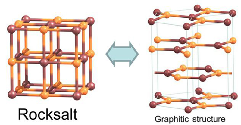
Transition from a cubic arrangement into several hexagonal layers. Image: Moscow Institute of Physics and Technology
An international collaborative of researchers has used computer simulations to find the minimum thinness of a slab of salt in order for it to break up into graphene-like layers. Based on the computer simulation, they derived the equation for the number of layers in a crystal that will produce ultrathin films with applications in nanoelectronics. Their findings are published in The Journal of Physical Chemistry Letters.
Unique monoatomic thickness of graphene makes it an attractive and useful material. Its crystal lattice resembles a honeycomb, as the bonds between the constituent atoms form regular hexagons. Graphene is a single layer of a three-dimensional graphite crystal and its properties (as well as properties of any 2D crystal) are radically different from its 3D counterpart. Since the discovery of graphene, a large amount of research has been directed at new two-dimensional materials with intriguing properties. Ultrathin films have unusual properties that might be useful for applications such as nano- and microelectronics.
Previous theoretical studies have suggested that films with a cubic structure and ionic bonding could spontaneously convert to a layered hexagonal graphitic structure in what is known as graphitization. For some substances, this conversion has been experimentally observed. It was predicted that rock salt NaCl could be a compound with graphitization tendencies. Graphitization of cubic compounds could produce new and promising structures for applications in nanoelectronics. However, no theory has accounted for this process with an arbitrary cubic compound or made predictions about its conversion into graphene-like salt layers.
For graphitization to occur, the crystal layers need to be reduced along the main diagonal of the cubic structure. This would result in one crystal surface being made of sodium ions and the other of chloride ions. It is important to note that positive and negative ions — and not neutral atoms — occupy the lattice points of the structure. This generates charges of opposite signs on the two surfaces. As long as the surfaces are remote from each other, all charges cancel out, and the salt slab shows a preference for a cubic structure. However, a sufficiently thin film gives rise to a large dipole moment due to the opposite charges of the two crystal surfaces. The structure seeks to get rid of the dipole moment, which increases the energy of the system. To make the surfaces charge-neutral, the crystal undergoes a rearrangement of atoms.
To study how graphitization tendencies vary depending on the compound, the researchers examined 16 binary compounds with the general formula AB, where A stands for one of the four alkali metals lithium Li, sodium Na, potassium K, and rubidium Rb. These are highly reactive elements found in Group 1 of the periodic table. The B in the formula stands for any of the four halogens fluorine F, chlorine Cl, bromine Br, and iodine I. These elements are in Group 17 of the periodic table and readily react with alkali metals.
All compounds in this study come in a number of structures, also known as crystal lattices or phases. If atmospheric pressure is increased to 300,000 times its normal value, another phase (B2) of NaCl (represented by the yellow portion of the diagram) becomes more stable, effecting a change in the crystal lattice. To test their choice of methods and parameters, the researchers simulated two crystal lattices and calculated the pressure that corresponds to the phase transition between them. Their predictions agree with experimental data.
The compounds within the scope of this study can all have a hexagonal, “graphitic” G phase (the red in the diagram) that is unstable in 3D bulk but becomes the most stable structure for ultrathin (2D or quasi-2D) films. The researchers identified the relationship between the surface energy of a film and the number of layers in it for both cubic and hexagonal structures. They graphed this relationship by plotting two lines with different slopes for each of the compounds studied. Each pair of lines associated with one compound has a common point that corresponds to the critical slab thickness that makes conversion from a cubic to a hexagonal structure energetically favorable. For example, the critical number of layers was found to be close to 11 for all sodium salts and between 19 and 27 for lithium salts.
Based on this data, the researchers established a relationship between the critical number of layers and two parameters that determine the strength of the ionic bonds in various compounds. The first parameter indicates the size of an ion of a given metal — its ionic radius. The second parameter is called electronegativity and is a measure of the atom’s ability to attract the electrons of element B. Higher electronegativity means more powerful attraction of electrons by the atom, a more pronounced ionic nature of the bond, a larger surface dipole, and a lower critical slab thickness.
Pavel Sorokin, head of the Laboratory of New Materials Simulation at TISNCM says, “This work has already attracted our colleagues from Israel and Japan. If they confirm our findings experimentally, this phenomenon [of graphitization] will provide a viable route to the synthesis of ultrathin films with potential applications in nanoelectronics.”
The scientists intend to broaden the scope of their studies by examining other compounds. They believe that ultrathin films of different composition might also undergo spontaneous graphitization, yielding new layered structures with properties that are even more intriguing.